At its core, an electron beam is a tool for delivering highly concentrated energy with extreme precision. It functions by accelerating a stream of electrons to high velocities and focusing them onto a tiny spot. This capability makes it indispensable for a range of advanced industrial and scientific tasks, from high-performance welding, as used in aerospace since the 1950s, to manufacturing the microchips in modern electronics.
An electron beam's true value lies in its ability to be precisely controlled by electric and magnetic fields. This allows it to manipulate or image materials at a microscopic level, making it a foundational technology for processes that demand unparalleled accuracy and energy density.
The Core Principle: Focused Energy and Precision
The utility of an electron beam stems from the fundamental properties of electrons and our ability to manipulate them.
High Energy Density
Electrons are accelerated to a significant fraction of the speed of light, imbuing them with high kinetic energy. When this beam strikes a material, that energy is converted into intense, localized heat.
This process can generate power densities millions of times greater than a conventional flame, allowing it to instantly melt or vaporize any known material in a highly controlled manner.
Precise Control and Steering
Because electrons are charged particles, their path can be deflected and focused with incredible accuracy using magnetic lenses.
This allows the beam to be steered in complex patterns with micrometer-level precision, essentially acting as a microscopic tool for cutting, etching, or welding.
Operation in a Vacuum
To be effective, the process must occur in a vacuum. Air molecules would otherwise scatter the electrons, diffusing the beam and drastically reducing its energy density and precision.
This is why industrial systems, such as welders, are built with working vacuum chambers ranging from small enclosures to massive rooms.
Key Industrial and Scientific Applications
The unique properties of electron beams enable several critical high-tech applications that would otherwise be impossible.
Electron Beam Welding (EBW)
As mentioned in early industrial use, EBW uses the beam's intense heat to create deep, narrow, and exceptionally strong welds.
Because the heat is so localized, the surrounding material is not significantly affected. This minimizes distortion and thermal stress, making it ideal for joining delicate or high-performance components in the aerospace, automotive, and medical industries. Systems can deliver up to 100 kW of power for heavy-duty applications.
Electron Beam Lithography (EBL)
This same precision is used to manufacture microchips. In EBL, the electron beam acts like an ultra-fine pen, drawing circuit patterns with nanoscale dimensions onto a silicon wafer coated with a sensitive material called a resist.
This process is fundamental to creating the masks used for mass-producing the most advanced processors and memory chips.
Scanning Electron Microscopy (SEM)
Instead of destroying the material, a lower-energy electron beam can be used for imaging. An SEM scans a beam across a sample's surface, causing it to emit secondary electrons.
Detectors capture these secondary electrons to form a highly detailed, three-dimensional-like image of the surface topography. This technique is invaluable in materials science, biology, and forensics for examining microscopic structures.
Sterilization and Material Curing
A high-energy electron beam can penetrate materials and break the DNA of microorganisms without significant heating. This makes it an effective method for the rapid sterilization of pre-packaged medical devices and food products.
Similarly, the beam's energy can be used to instantly cure or harden inks, adhesives, and coatings in a process known as E-beam curing.
Understanding the Trade-offs
While powerful, electron beam technology has inherent limitations that define where it can be applied effectively.
The Vacuum Requirement
The need for a vacuum is the most significant operational constraint. It increases equipment cost and complexity, and it limits the size of the object that can be processed. This makes it less suitable for very large structures or low-cost, high-volume production where other methods suffice.
Generation of X-rays
When high-energy electrons strike a dense material, their rapid deceleration produces X-rays (a phenomenon known as Bremsstrahlung). This requires substantial lead or concrete shielding to protect operators, adding significant cost, weight, and facility requirements to the system.
High Capital Cost
The combination of a high-voltage power supply, vacuum system, electron gun, and safety shielding makes electron beam equipment expensive. Its use is typically justified only for high-value applications where the precision, performance, or unique capabilities cannot be achieved by other means.
Making the Right Choice for Your Goal
Deciding if an electron beam is the appropriate tool depends entirely on the specific requirements of your application.
- If your primary focus is joining high-performance materials: E-beam welding provides superior strength and minimal distortion for critical components in aerospace and medical devices.
- If your primary focus is creating nanoscale patterns: E-beam lithography is the gold standard for prototyping and producing masks for advanced semiconductors.
- If your primary focus is imaging microscopic surfaces: A Scanning Electron Microscope offers unmatched resolution and depth of field for detailed topographical analysis.
- If your primary focus is industrial-scale processing: E-beam sterilization and curing offer speed and efficiency for high-value products like medical supplies and advanced composites.
Ultimately, electron beams provide an unparalleled level of precision, making them indispensable for tasks that demand microscopic control over energy and matter.
Summary Table:
| Application | Key Benefit | Primary Industries |
|---|---|---|
| Electron Beam Welding (EBW) | Deep, strong welds with minimal distortion | Aerospace, Automotive, Medical |
| Electron Beam Lithography (EBL) | Nanoscale patterning for microchips | Semiconductor, Electronics |
| Scanning Electron Microscopy (SEM) | High-resolution surface imaging | Materials Science, Biology, Forensics |
| Sterilization & Curing | Rapid, non-thermal processing | Medical Devices, Food, Composites |
Ready to leverage electron beam precision in your lab? KINTEK specializes in high-performance lab equipment and consumables, delivering the advanced tools you need for electron beam applications, from welding to microscopy. Our expertise ensures you get the right solutions for your specific industrial or research challenges. Contact us today to discuss how we can support your laboratory's success!
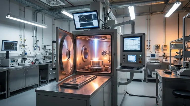
Visual Guide

Related Products
- Electron Beam Evaporation Coating Tungsten Crucible and Molybdenum Crucible for High Temperature Applications
- Electron Beam Evaporation Coating Oxygen-Free Copper Crucible and Evaporation Boat
- E Beam Crucibles Electron Gun Beam Crucible for Evaporation
- Electron Beam Evaporation Coating Gold Plating Tungsten Molybdenum Crucible for Evaporation
- Electron Beam Evaporation Coating Conductive Boron Nitride Crucible BN Crucible
People Also Ask
- What is the deposition rate of e-beam evaporation? Control Thin Film Quality and Speed
- What materials are used in electron beam evaporation? Master High-Purity Thin Film Deposition
- What is the process of e-beam coating? Achieve High-Purity, Precise Thin Films for Your Lab
- What is the temperature of e-beam evaporation? Mastering the Two-Zone Thermal Process for Precision Films
- What is the container that holds the metal source material called in e-beam evaporation? Ensure Purity and Quality in Your Thin-Film Deposition


