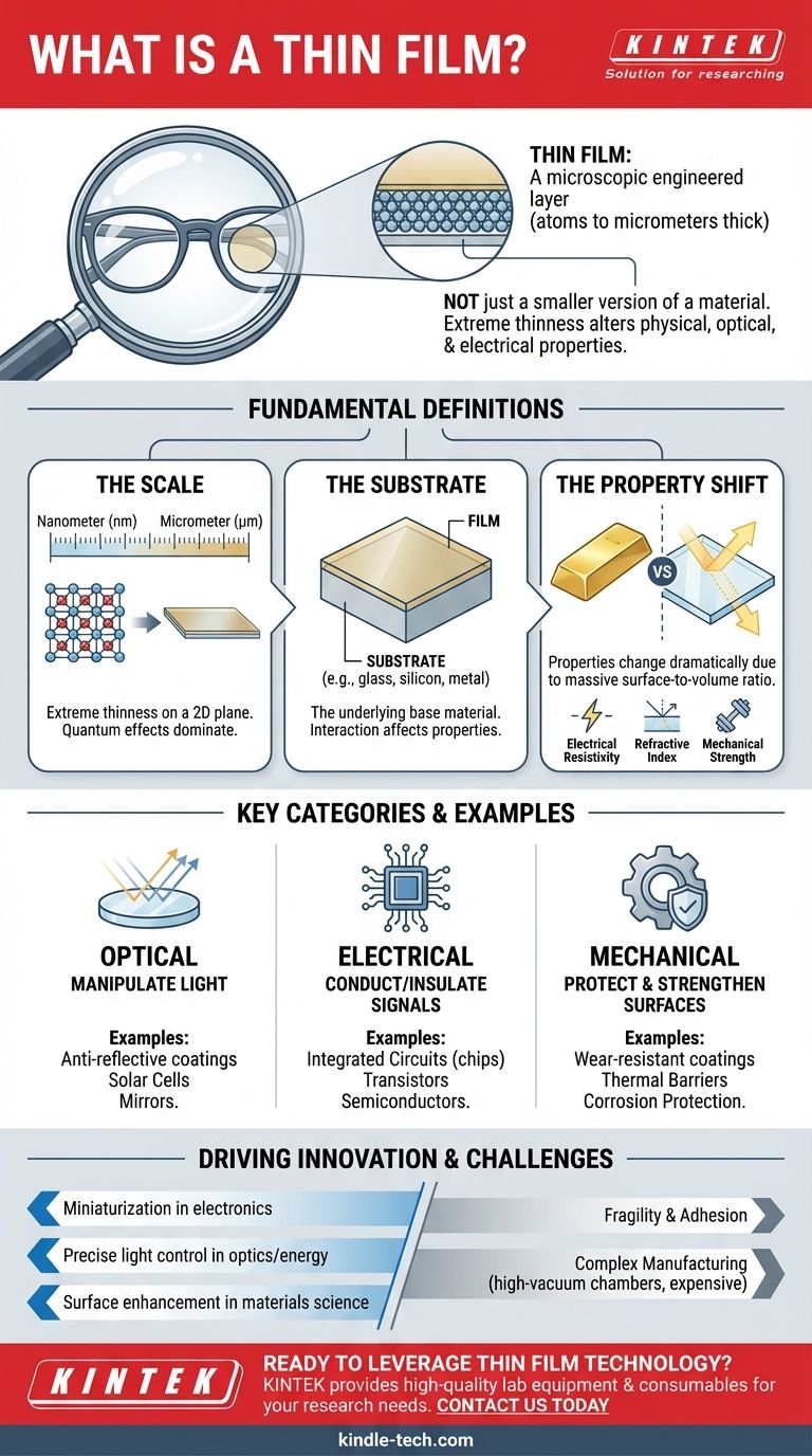
In essence, a thin film is a microscopic layer of material, ranging from a few atoms to several micrometers in thickness, intentionally deposited onto a surface called a substrate. These engineered layers are fundamental to modern technology, forming the basis for everything from the anti-reflective coating on your eyeglasses to the complex circuitry inside your smartphone.
A thin film is not merely a smaller version of a material. Its extreme thinness, where the surface-to-volume ratio is massive, fundamentally alters its physical, optical, and electrical properties, enabling capabilities that are impossible with the bulk material.
What Fundamentally Defines a Thin Film?
To grasp the importance of thin films, we must look beyond the simple definition and understand the core principles that give them their unique power.
The Scale: From Microns to Atoms
The defining characteristic of a thin film is its thickness, which is suppressed to the nanometer (billionths of a meter) or micrometer (millionths of a meter) scale.
This extreme thinness means the film is essentially a two-dimensional plane. At this scale, quantum effects and surface interactions begin to dominate the material's behavior.
The Substrate: A Necessary Foundation
A thin film does not exist in isolation. It is always applied to a substrate, which is the underlying base material like glass, silicon, or metal.
The interaction between the film and the substrate is critical, affecting everything from adhesion and stability to the film's final properties.
The Property Shift: Beyond Bulk Material
This is the most critical concept. A one-micrometer thick layer of gold does not behave like a solid gold bar.
Because so many of its atoms are at or near a surface, the film's electrical resistivity, index of refraction, and mechanical strength change dramatically. We engineer thin films specifically to harness these novel properties.
Key Categories and Real-World Examples
Thin films are typically categorized by their application, as their properties are tailored for a specific function.
Optical Thin Films
These films are designed to manipulate light. The thickness of the film is precisely controlled, often relative to the wavelength of light, to cause interference effects.
Common examples include anti-reflective coatings on camera lenses and monitors, reflective coatings for mirrors, and the light-absorbing layers in solar cells.
Electrical Thin Films
These form the backbone of all modern electronics. Complex devices are built by layering different types of films on a silicon wafer.
Integrated circuits (computer chips) are the ultimate example, containing billions of transistors built from stacked thin films of conducting, insulating, and semiconducting materials.
Mechanical Thin Films
These films are engineered to enhance the surface of a material, often for protection. They are typically made of extremely hard and inert materials.
Applications include wear-resistant coatings on cutting tools and engine parts, corrosion-resistant layers in aerospace components, and thermal barriers for jet engine turbines.
Understanding the Trade-offs
While powerful, the nature of thin films also presents significant engineering challenges.
Fragility and Adhesion
By their very nature, thin films can be delicate and susceptible to scratches, peeling, or damage from environmental factors.
Ensuring the film adheres strongly and permanently to its substrate is a major challenge in manufacturing and a common point of failure.
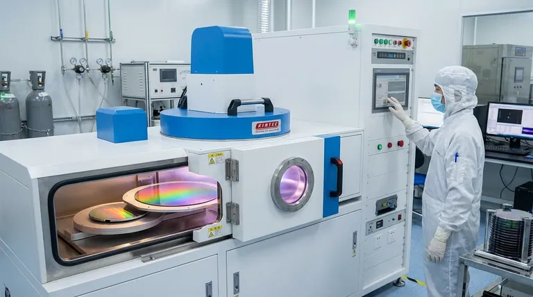
Complex Manufacturing
Creating a uniform film that is only a few hundred atoms thick requires highly controlled conditions and sophisticated equipment.
Processes like sputtering or chemical vapor deposition occur in high-vacuum chambers and require high-purity materials, making the manufacturing process complex and expensive.
How Thin Films Drive Innovation
Understanding the function of thin films allows you to see their central role in nearly every field of technology.
- If your primary focus is electronics and computing: Recognize that the relentless miniaturization of devices is entirely dependent on our ability to deposit and pattern increasingly complex layers of electrical thin films.
- If your primary focus is optics and energy: Understand that thin films give us precise control over light, enabling everything from high-efficiency solar panels to advanced optical sensors and displays.
- If your primary focus is materials science and engineering: View thin films as a powerful tool for enhancing the surface properties of a bulk material, adding functions like hardness or corrosion resistance without altering the core component.
Ultimately, mastering the art of the thin film is central to pushing the boundaries of modern technology.
Summary Table:
| Category | Primary Function | Key Examples |
|---|---|---|
| Optical | Manipulate Light | Anti-reflective coatings, solar cells, mirrors |
| Electrical | Conduct/Insulate Signals | Integrated circuits, transistors, semiconductors |
| Mechanical | Protect & Strengthen Surfaces | Wear-resistant coatings, thermal barriers, corrosion protection |
Ready to leverage thin film technology in your lab? At KINTEK, we specialize in providing high-quality lab equipment and consumables for all your thin film research and production needs. Whether you're developing advanced electronics, optical sensors, or protective coatings, our solutions ensure precision and reliability. Contact us today to discuss how we can support your innovation journey!
Visual Guide
Related Products
- Aluminum-Plastic Flexible Packaging Film for Lithium Battery Packaging
- Thin-Layer Spectral Electrolysis Electrochemical Cell
People Also Ask
- What are the three types of lamination? Choose the Perfect Finish for Your Print Project
- Is there a way to test lithium batteries? Understand Voltage vs. True Health
- What are the properties of Aluminium (Al) relevant to its use in coatings? High Reflectivity & Conductivity Explored
- What is organic thin film? A Guide to Engineered Molecular Layers for Advanced Tech
- How to check if a lithium battery is good? Safely Test Voltage, Capacity & Internal Resistance

