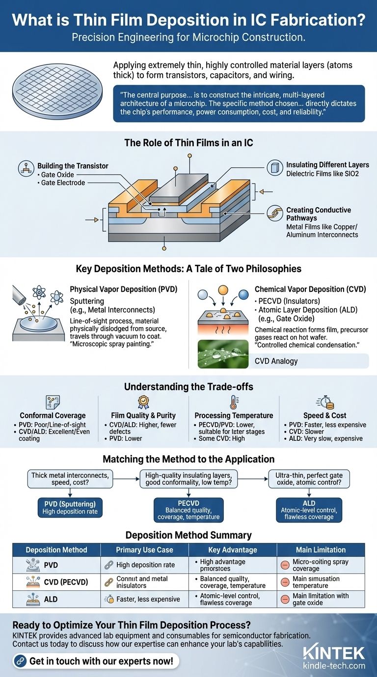
At its core, thin film deposition in IC fabrication is the process of applying an extremely thin, highly controlled layer of material onto a semiconductor wafer. These layers, often just a few atoms thick, can be conductive, insulating, or semiconducting, forming the fundamental building blocks of the transistors, capacitors, and wiring that make up a microchip. This is not simply coating a surface; it is a precision engineering process that defines the electrical characteristics and physical structure of the entire circuit.
The central purpose of thin film deposition is to construct the intricate, multi-layered architecture of a microchip. The specific method chosen—whether physical or chemical—is a critical decision that directly dictates the chip's performance, power consumption, cost, and reliability.
The Role of Thin Films in an IC
A modern integrated circuit is a three-dimensional structure built from dozens, sometimes hundreds, of stacked layers. Thin film deposition is the technique used to create most of these layers.
Building the Transistor
The transistor, the basic switch in a computer, relies entirely on deposited films. An ultra-thin insulating layer (gate oxide) is deposited to control the flow of electricity, and a conductive layer (gate electrode) is deposited on top of it to act as the switch.
Insulating Different Layers
With millions of transistors packed together and multiple levels of wiring, preventing electrical "short circuits" is critical. Dielectric films (insulators) like silicon dioxide are deposited between conductive layers to isolate them from each other.
Creating Conductive Pathways
After the transistors are formed, they must be connected. This is done by depositing metal films, such as copper or aluminum, to create a complex network of wires known as interconnects.
Key Deposition Methods: A Tale of Two Philosophies
Deposition techniques are broadly categorized into two families based on how they move material from a source to the wafer: physically or chemically.
Physical Vapor Deposition (PVD)
PVD is a line-of-sight process where a material is physically dislodged from a source and travels through a vacuum to coat the wafer. Think of it as a microscopic form of spray painting with atoms.
The most common PVD method is sputtering, where high-energy ions bombard a source "target," knocking atoms loose that then deposit onto the wafer. It is excellent for depositing metals for interconnects.
Chemical Vapor Deposition (CVD)
CVD uses a chemical reaction to form the film. Precursor gases are introduced into a chamber, where they react on the hot wafer surface to create a solid layer, leaving behind volatile byproducts that are pumped away.
This is analogous to how dew forms on a cold surface, but instead of simple condensation, it's a controlled chemical reaction creating a new, engineered material. Common variants like Plasma-Enhanced CVD (PECVD) use plasma to enable these reactions at lower temperatures.
Atomic Layer Deposition (ALD)
ALD is an advanced, highly precise subtype of CVD. It builds the film literally one atomic layer at a time through a sequence of self-limiting chemical reactions.
While extremely slow, ALD provides unparalleled control over film thickness and the ability to perfectly coat even the most complex, three-dimensional microscopic structures.
Understanding the Trade-offs
No single deposition method is universally superior. The choice is always a matter of balancing competing requirements for the specific layer being built.
Conformal Coverage (Step Coverage)
This refers to a film's ability to evenly coat vertical sidewalls and deep trenches. CVD and ALD excel here, as the chemical reactions occur on all exposed surfaces. PVD is a line-of-sight process and struggles to coat complex topographies, resulting in thinner coverage on sidewalls.
Film Quality and Purity
CVD and ALD generally produce films with higher purity and fewer structural defects than PVD. The chemical nature of the process allows for greater control over the film's final composition and properties.
Processing Temperature
The temperature at which deposition occurs is a major constraint. High temperatures can damage structures already built on the wafer. While some CVD processes require very high heat, PECVD and PVD operate at lower temperatures, making them suitable for later stages of fabrication.
Speed and Cost
PVD is typically a faster and less expensive process than CVD, making it ideal for depositing thicker metal layers where absolute perfection is not the primary goal. ALD is by far the slowest and most expensive method, reserved only for the most critical, ultra-thin layers.
Matching the Method to the Application
Your choice of deposition technique is dictated entirely by the function of the layer you are creating.
- If your primary focus is creating thick metal interconnects quickly and cost-effectively: PVD (sputtering) is the standard industry choice due to its high deposition rate.
- If your primary focus is depositing high-quality insulating layers between metal lines: PECVD offers an excellent balance of film quality, conformal coverage, and a low processing temperature.
- If your primary focus is building an ultra-thin, perfectly uniform gate oxide for a leading-edge transistor: ALD is the only method that provides the required atomic-level control and flawless coverage.
Choosing the right deposition process is a foundational skill in semiconductor engineering, enabling the creation of ever more powerful and efficient microchips.
Summary Table:
| Deposition Method | Primary Use Case | Key Advantage | Main Limitation |
|---|---|---|---|
| PVD (Sputtering) | Metal interconnects | High speed, cost-effective | Poor conformal coverage |
| CVD (PECVD) | Insulating layers | Good conformality, lower temperature | Slower than PVD |
| ALD | Ultra-thin critical layers (e.g., gate oxide) | Atomic-level control, perfect conformity | Very slow, high cost |
Ready to Optimize Your Thin Film Deposition Process?
The right equipment is critical for achieving the precise, high-quality layers that define modern microchips. At KINTEK, we specialize in providing advanced lab equipment and consumables for semiconductor fabrication, including state-of-the-art deposition systems.
Whether you are developing next-generation transistors or refining your interconnect technology, our solutions are designed to meet the stringent demands of IC manufacturing. Contact us today to discuss how our expertise can enhance your lab's capabilities and drive your projects forward.
Get in touch with our experts now!
Visual Guide
Related Products
- Aluminized Ceramic Evaporation Boat for Thin Film Deposition
- Tungsten Evaporation Boat for Thin Film Deposition
- Electron Beam Evaporation Coating Oxygen-Free Copper Crucible and Evaporation Boat
- Molybdenum Tungsten Tantalum Evaporation Boat for High Temperature Applications
- HFCVD Machine System Equipment for Drawing Die Nano-Diamond Coating
People Also Ask
- Why is an alumina boat and Ti3AlC2 powder bed necessary for Ti2AlC sintering? Protect MAX Phase Purity
- What are thin films deposited by evaporation? A Guide to High-Purity Coating
- What is thin film deposition? Unlock Advanced Surface Engineering for Your Materials
- What is the widely used boat made of in thermal evaporation? Choosing the Right Material for High-Purity Deposition
- What is the source of evaporation for thin film? Choosing Between Thermal and E-Beam Methods


