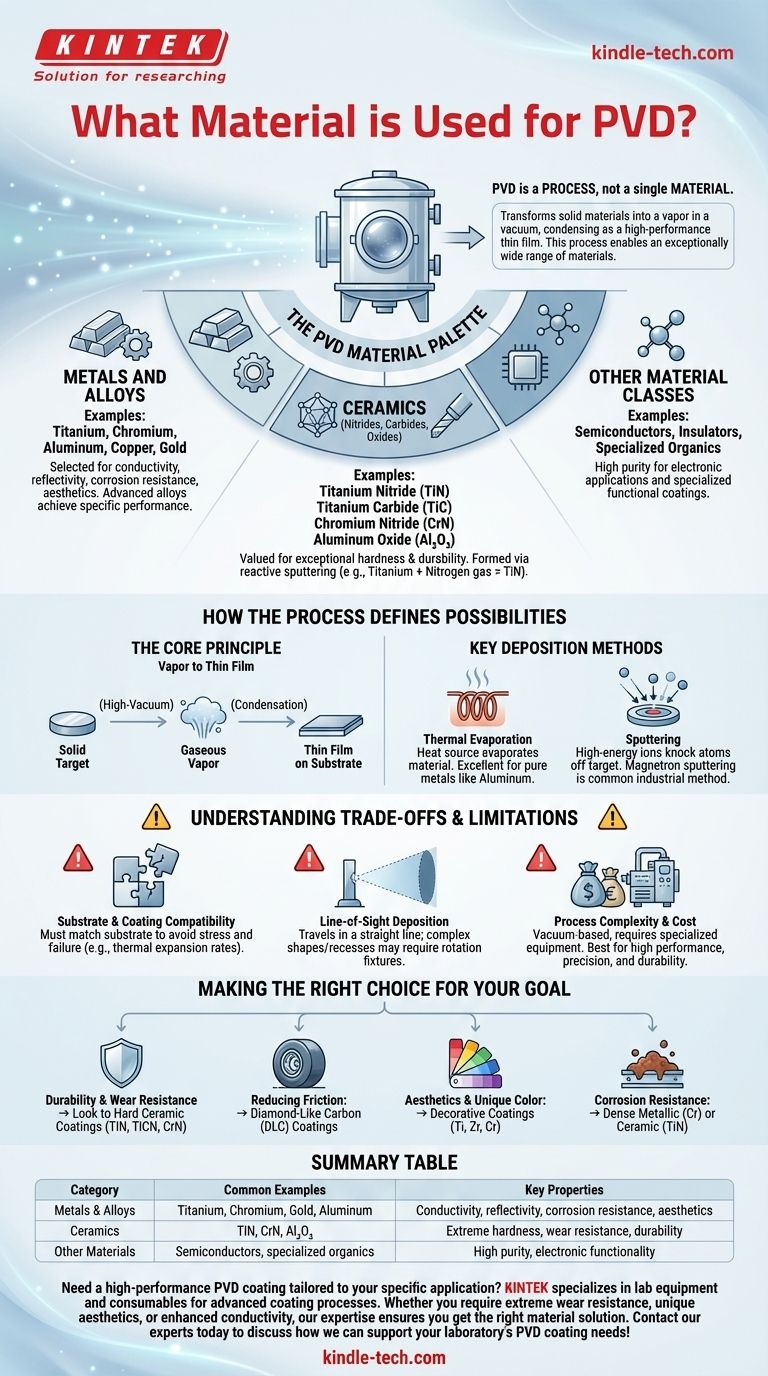
In essence, Physical Vapor Deposition (PVD) is not limited to one specific material but is a process capable of depositing nearly any inorganic and some organic materials. The most common materials used for PVD coatings are metals, metal alloys, and ceramics, such as oxides, nitrides, and carbides. This versatility allows the final coating's properties—like hardness, color, and conductivity—to be precisely engineered for a specific function.
PVD is best understood not by the material it uses, but by the process it enables. It transforms solid materials into a vapor within a vacuum, which then condenses onto a part's surface as a high-performance thin film. This core principle is what allows for an exceptionally wide range of coating materials.
The PVD Material Palette: From Pure Metals to Advanced Ceramics
The strength of PVD lies in its ability to handle a diverse catalog of source materials. These materials are chosen based on the desired properties of the final coating.
Metals and Alloys
Pure metals and alloys are foundational materials for PVD. They are selected for properties ranging from conductivity and reflectivity to corrosion resistance and aesthetics.
Common examples include Titanium, Chromium, Aluminum, Copper, and Gold. Advanced alloys, such as those containing combinations of chromium and iron, can also be deposited to achieve specific performance characteristics not found in a single metal.
Ceramics (Nitrides, Carbides, and Oxides)
Ceramics represent one of the most important classes of PVD coatings, valued for their exceptional hardness and durability. These are not deposited as pre-made ceramics; instead, they are formed during the process.
This is often achieved through reactive sputtering, where a reactive gas like nitrogen or oxygen is introduced into the vacuum chamber. This gas reacts with the vaporized metal (like titanium) to form a ceramic compound directly on the substrate's surface.
The most well-known example is Titanium Nitride (TiN), prized for its gold color and extreme wear resistance on cutting tools and industrial parts. Other common ceramics include Titanium Carbide (TiC), Chromium Nitride (CrN), and Aluminum Oxide (Al₂O₃).
Other Material Classes
Beyond metals and ceramics, PVD's capabilities extend to other advanced materials. This includes semiconductors and insulators, which can be deposited with high purity for electronic applications. While less common, certain organic materials can also be deposited using specialized PVD techniques.
How the Process Defines the Possibilities
The reason PVD can use so many different materials is because of its fundamental mechanism. The process is not chemical; it is physical.
The Core Principle: Vapor to Thin Film
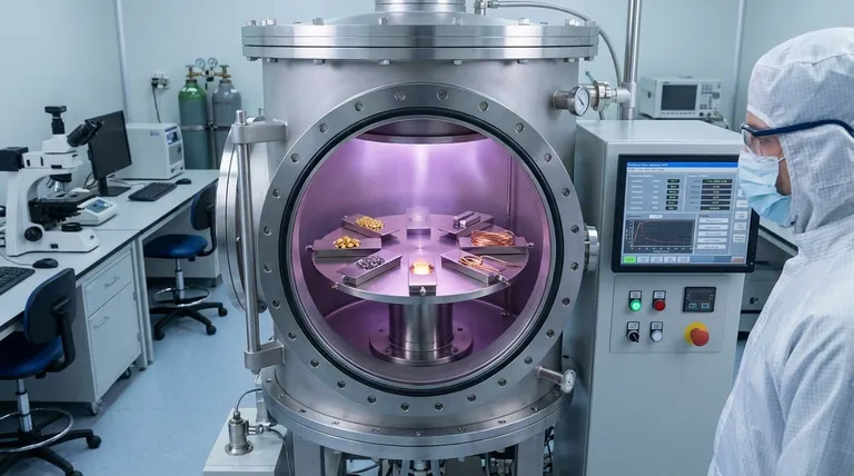
All PVD methods share a common sequence. First, a solid source material (known as the target) is converted into a gaseous vapor phase. This is done inside a high-vacuum chamber.
Second, this vapor travels through the chamber and condenses onto the substrate (the part being coated), forming a thin, uniform, and highly adherent film.
Key Deposition Methods
The main difference between PVD techniques lies in how they create the vapor.
- Thermal Evaporation: The source material is heated by an electric heater or an electron beam until it evaporates into the gas phase. This method is excellent for creating extremely pure films of metals like aluminum.
- Sputtering: The source material is bombarded with high-energy ions, which physically knock atoms off the target. This "sputtered" material then deposits onto the substrate. Magnetron sputtering uses powerful magnets to increase the efficiency of this process and is the most common industrial method.
Understanding the Trade-offs and Limitations
While incredibly versatile, PVD is not a universal solution. Understanding its limitations is key to using it effectively.
Substrate and Coating Compatibility
The chosen coating material must be compatible with the substrate material. While PVD creates excellent adhesion, factors like different thermal expansion rates between the coating and the part can create stress and potential failure.
Line-of-Sight Deposition
Most PVD processes are "line-of-sight," meaning the coating material travels in a straight line from the source to the part. Complex shapes with deep recesses or hidden internal surfaces can be very difficult to coat uniformly without sophisticated fixtures that rotate the part during deposition.
Process Complexity and Cost
PVD is a vacuum-based process that requires expensive, specialized equipment. It is not typically the cheapest coating method and is best reserved for applications where high performance, precision, and durability justify the investment.
Making the Right Choice for Your Goal
The best PVD material is entirely dependent on your objective. Use your end goal to guide your material selection.
- If your primary focus is durability and wear resistance: Look to hard ceramic coatings like Titanium Nitride (TiN), Titanium Carbonitride (TiCN), or Chromium Nitride (CrN).
- If your primary focus is reducing friction: Diamond-Like Carbon (DLC) coatings, another PVD-applied family of materials, offer exceptional lubricity.
- If your primary focus is aesthetics and unique color: Decorative coatings using Titanium, Zirconium, and Chromium can produce a stable, brilliant spectrum of colors.
- If your primary focus is corrosion resistance: A dense, non-porous metallic coating like Chromium or a ceramic like TiN can provide an excellent barrier against environmental damage.
By understanding that PVD is a versatile process rather than a single material, you can engineer a surface with the precise properties your application demands.
Summary Table:
| Material Category | Common Examples | Key Properties |
|---|---|---|
| Metals & Alloys | Titanium, Chromium, Gold, Aluminum | Conductivity, reflectivity, corrosion resistance, aesthetics |
| Ceramics | Titanium Nitride (TiN), Chromium Nitride (CrN), Aluminum Oxide | Extreme hardness, wear resistance, durability |
| Other Materials | Semiconductors, specialized organics | High purity, electronic functionality |
Need a high-performance PVD coating tailored to your specific application? KINTEK specializes in lab equipment and consumables for advanced coating processes. Whether you require extreme wear resistance, unique aesthetics, or enhanced conductivity, our expertise ensures you get the right material solution. Contact our experts today to discuss how we can support your laboratory's PVD coating needs!
Visual Guide
Related Products
- Hemispherical Bottom Tungsten Molybdenum Evaporation Boat
- Molybdenum Tungsten Tantalum Evaporation Boat for High Temperature Applications
- Aluminized Ceramic Evaporation Boat for Thin Film Deposition
- RF PECVD System Radio Frequency Plasma-Enhanced Chemical Vapor Deposition RF PECVD
- Tungsten Evaporation Boat for Thin Film Deposition
People Also Ask
- How is deposition time calculated? Mastering the Clock for Strategic Legal Advantage
- What is evaporation material? The Key to Precision Thin-Film Deposition
- What are the uses of evaporation in industry? From Food Concentration to High-Tech Thin Films
- What is the thermal evaporation technique? A Guide to Thin-Film Deposition for Your Lab
- What is thermal effect via evaporation? A Simple Guide to Thin-Film Deposition