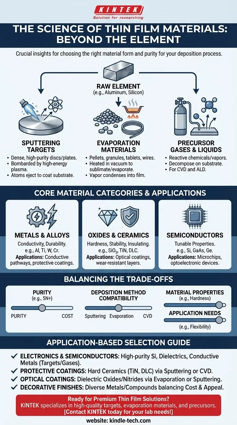
In thin film deposition, the primary materials used fall into broad categories including metals, oxides, ceramics, and semiconductor compounds. Specific examples range from elemental materials like aluminum (Al), titanium (Ti), and silicon (Si) to more complex compounds like titanium nitride (TiN) and gallium arsenide (GaAs), each chosen for its unique physical and chemical properties.
The critical insight is that the "material" is not just the chemical element or compound itself. It is the highly pure, specially processed form of that material—such as a sputtering target, an evaporation pellet, or a precursor gas—that is engineered for a specific deposition process and end application.
The Core Material Categories Explained
The selection of a thin film material is dictated entirely by the desired properties of the final layer, whether it's for electrical conductivity, optical transparency, or physical hardness.
Metals and Alloys
Metals are fundamental to many thin film applications, particularly in electronics for creating conductive pathways and in protective coatings for their durability.
Common metals include aluminum (Al), chromium (Cr), and titanium (Ti), as well as refractory metals like tungsten. Alloys are also used to fine-tune properties like resistance or hardness.
Oxides and Ceramics
This category includes materials known for their hardness, high-temperature stability, and dielectric (electrically insulating) properties. They are cornerstones of both optical coatings and semiconductor device fabrication.
Materials like silicon oxides and nitrides (e.g., titanium nitride - TiN) are frequently used. More advanced ceramics like diamond-like carbon (DLC) offer exceptional hardness and low friction for demanding wear-resistant applications.
Semiconductors
Semiconductor materials are the foundation of the entire electronics industry. Thin film deposition is a primary method for building the complex, layered structures of modern microchips.
Silicon (Si) is the most common semiconductor material. However, germanium (Ge) and compound semiconductors like gallium arsenide (GaAs) are used for specialized high-frequency or optoelectronic devices.
From Raw Material to Deposition-Ready Form
You do not simply use a block of metal or a pile of sand for thin film deposition. Raw materials are refined to extreme purity and shaped into a form compatible with a specific deposition technique.
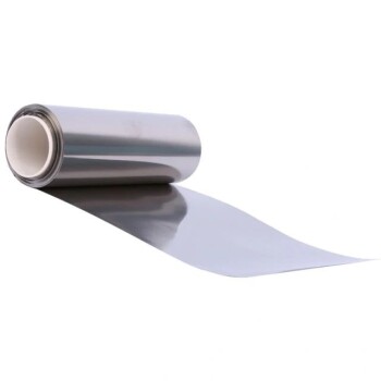
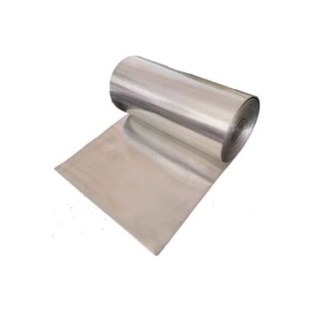
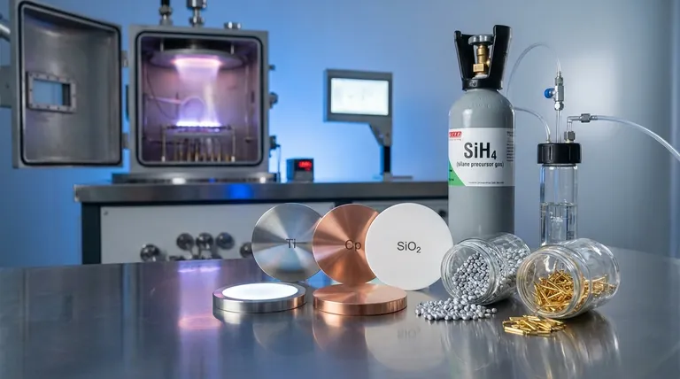
Sputtering Targets
For sputtering processes, materials are formed into dense, high-purity discs or plates called sputtering targets. A high-energy plasma bombards this target, ejecting atoms that then coat the substrate. The quality and purity of the target directly impact the quality of the film.
Evaporation Materials
For thermal or electron-beam evaporation, materials are supplied as pellets, granules, tablets, or wires. These are heated in a vacuum chamber until they sublimate or evaporate, with the resulting vapor condensing on the substrate to form the film.
Precursor Gases and Liquids
For methods like Chemical Vapor Deposition (CVD) and Atomic Layer Deposition (ALD), the source material is a chemical precursor. These are reactive gases or vaporized liquids that decompose on the substrate surface, leaving behind the desired material and releasing volatile byproducts.
Understanding the Trade-offs
Choosing a material involves balancing performance, cost, and process compatibility. An expert decision requires weighing these factors objectively.
Purity vs. Cost
For semiconductor applications, material purity of 99.999% (5N) or higher is non-negotiable, as even trace impurities can ruin a device. For a simple decorative coating, a lower-purity, less expensive material is often sufficient.
Deposition Method Compatibility
Not every material is suitable for every deposition method. Refractory metals with extremely high melting points are difficult to deposit using thermal evaporation but are well-suited for sputtering. Similarly, complex compounds may only be achievable through CVD.
Material Properties vs. Application Needs
The final choice is always a compromise. A metal may offer great conductivity but corrodes easily. An oxide may be extremely hard but also brittle. The goal is to select the material whose strengths align with the application's most critical requirements.
Selecting the Right Material for Your Goal
Your application dictates your material choice. To simplify this decision, consider your primary objective.
- If your primary focus is electronics and semiconductors: Prioritize high-purity silicon, dielectrics, and conductive metals supplied as sputtering targets or precursor gases.
- If your primary focus is protective or wear-resistant coatings: Consider hard ceramics like titanium nitride (TiN) or diamond-like carbon (DLC), often applied via sputtering or CVD.
- If your primary focus is optical coatings: Look to dielectric oxides and nitrides with specific refractive indices, typically deposited via evaporation or sputtering.
- If your primary focus is decorative finishes: A wider range of metals and compounds at lower purities can be used, often prioritizing cost-effectiveness and visual appeal.
Ultimately, the right material choice is a strategic decision that balances physical properties, deposition method, and the specific demands of your final product.
Summary Table:
| Material Category | Common Examples | Key Properties | Primary Applications |
|---|---|---|---|
| Metals & Alloys | Aluminum (Al), Titanium (Ti), Tungsten (W) | High electrical conductivity, durability | Conductive pathways, protective coatings |
| Oxides & Ceramics | Silicon Dioxide (SiO₂), Titanium Nitride (TiN) | Hardness, high-temperature stability, insulating | Optical coatings, wear-resistant layers |
| Semiconductors | Silicon (Si), Gallium Arsenide (GaAs) | Tunable electrical properties | Microchips, optoelectronic devices |
| Deposition Forms | Sputtering Targets, Evaporation Pellets, Precursor Gases | Varies by process (e.g., high purity for sputtering) | Compatible with specific techniques like PVD or CVD |
Ready to Source the Right Thin Film Materials?
Choosing the correct high-purity material in the proper form is critical to your project's success. KINTEK specializes in providing premium lab equipment and consumables, including high-quality sputtering targets, evaporation materials, and precursor gases tailored for your specific deposition process and application—whether it's for semiconductors, protective coatings, or optical layers.
Our experts can help you navigate the trade-offs between material properties, purity, and cost to ensure optimal performance.
Let's discuss your project requirements. Contact our team today to find the perfect thin film solution for your laboratory needs!
Visual Guide
Related Products
- HFCVD Machine System Equipment for Drawing Die Nano-Diamond Coating
- CVD Diamond Cutting Tool Blanks for Precision Machining
- 915MHz MPCVD Diamond Machine Microwave Plasma Chemical Vapor Deposition System Reactor
- Vacuum Hot Press Furnace Machine for Lamination and Heating
- Custom Machined and Molded PTFE Teflon Parts Manufacturer for Laboratory ITO FTO Conductive Glass Cleaning Flower Basket
People Also Ask
- What machine is used to make lab-grown diamonds? Discover the HPHT & CVD Technologies
- What is direct current DC magnetron sputtering? A Guide to High-Quality Thin Film Deposition
- How is something diamond coated? A Guide to CVD Growth vs. Plating Methods
- How do you calculate coating coverage? A Practical Guide to Accurate Material Estimation
- What is microwave plasma CVD? A Guide to High-Purity Diamond and Material Synthesis