PECVD systems are primarily utilized for depositing silicon-based dielectric and semiconductor films. The three most specific and common types of films deposited are Silicon Dioxide (SiO2), Silicon Nitride (Si3N4), and Amorphous Silicon (a-Si).
Plasma Enhanced Chemical Vapor Deposition (PECVD) is the industry standard for creating thin films that require superior dielectric properties, low mechanical stress, and excellent conformal coverage, serving as the backbone for modern semiconductor isolation and encapsulation.
The Core Portfolio of PECVD Films
While the range of applications is broad, the specific films generated by these systems generally fall into two categories: standard silicon derivatives and specialized hard coatings.
Standard Silicon-Based Films
The primary reference highlights that the foundational films for this process are Silicon Dioxide (SiO2), Silicon Nitride (Si3N4), and Amorphous Silicon (a-Si).
These three materials form the basis of most semiconductor fabrication tasks, largely due to the interaction of process gases like silane and ammonia within the plasma.
Specialized and Hard Coatings
Beyond the standard silicon trio, supplementary data indicates that PECVD systems are capable of depositing more specialized materials.
These include Silicon Carbide, Diamond-like Carbon (DLC), and Poly-silicon.
Additionally, the process is used to deposit dopants and various forms of silicon oxides, expanding its utility beyond simple insulation.
Critical Properties Driving Film Selection
Engineers choose PECVD not just for the material itself, but for the specific physical qualities the process imparts to that material.
Electrical Isolation
Films deposited via PECVD, particularly oxides and nitrides, possess excellent dielectric properties.
This is essential for integrated circuit fabrication, where transistors require a high-quality dielectric layer to function correctly and conductive layers must be effectively isolated.
Mechanical Stability
A major advantage of these specific films is their low mechanical stress.
Low stress ensures the films do not deform, crack, or become non-uniform after deposition, which is vital for the structural integrity of the chip.
Conformal Coverage
PECVD films are known for excellent step coverage.
This means the film can uniformly coat complex, uneven topographies on a silicon chip, ensuring no gaps or weak points in the encapsulation or passivation layers.
Common Applications by Film Type
The specific film types mentioned above are applied to solve distinct challenges in manufacturing.
Semiconductor Protection
Silicon Dioxide and Silicon Nitride are heavily used for surface passivation and device encapsulation.
They protect the underlying circuitry from environmental damage and electrical interference.
Optical Enhancement
Certain PECVD films serve as anti-reflective layers in optical applications.
By controlling the chemical composition and thickness, engineers can tune the optical properties of the film.
Advanced Device Fabrication
These films are integral to Very Large-Scale Integrated (VLSI) circuits and Micro-Electro-Mechanical Systems (MEMS).
Their strong substrate adhesion makes them reliable for the microscopic moving parts found in MEMS devices.
Understanding Process Control Variables
While PECVD offers versatility, the quality of the specific film depends heavily on precise process control.
Tuning Composition and Thickness
The PECVD process occurs in a closed vacuum body using radio frequency to ionize gases.
Operators must carefully control this environment to dictate the thickness and chemical composition of the final film.
The Uniformity Factor
Achieving the "excellent uniformity" mentioned in technical literature requires rigorous management of the plasma environment.
Any deviation in gas flow or ionization levels can alter the physical properties of the deposited layer, potentially compromising the device.
Making the Right Choice for Your Goal
Selecting the specific film type depends entirely on the function the layer must serve within the device stack.
- If your primary focus is electrical isolation: Prioritize Silicon Dioxide (SiO2) or Silicon Nitride (Si3N4) for their superior dielectric properties and use in isolating conductive layers.
- If your primary focus is active semiconductor layers: Utilize Amorphous Silicon (a-Si) or Poly-silicon, which are standard for creating active device regions.
- If your primary focus is durability or optics: Consider Diamond-like Carbon or specialized anti-reflective coatings for mechanical hardness or light management.
By leveraging the low-stress and high-conformality characteristics of PECVD films, you ensure the long-term reliability of complex semiconductor devices.
Summary Table:
| Film Type | Chemical Formula | Key Properties | Primary Applications |
|---|---|---|---|
| Silicon Dioxide | SiO2 | High dielectric strength, excellent isolation | Gate dielectrics, interlayer insulation |
| Silicon Nitride | Si3N4 | High hardness, moisture barrier | Surface passivation, device encapsulation |
| Amorphous Silicon | a-Si | Tunable conductivity, low stress | Solar cells, TFTs, active device layers |
| Diamond-like Carbon | DLC | Exceptional hardness, low friction | Wear-resistant coatings, hard protective layers |
| Silicon Carbide | SiC | Chemical stability, thermal resistance | High-temperature electronics, MEMS |
Optimize Your Thin Film Deposition with KINTEK
Precision matters in semiconductor and material research. KINTEK specializes in high-performance laboratory equipment, providing advanced PECVD systems and specialized solutions like high-temperature furnaces (CVD, PECVD, MPCVD), vacuum systems, and high-pressure reactors to meet your exact thin-film requirements.
Whether you are developing next-generation MEMS or optimizing passivation layers, our team provides the tools and consumables (including ceramics and crucibles) necessary for superior uniformity and low mechanical stress.
Ready to elevate your lab's capabilities? Contact KINTEK today for expert guidance and tailored solutions!
Related Products
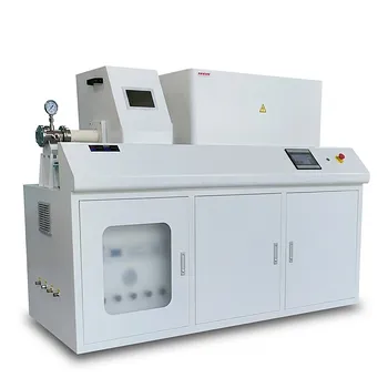
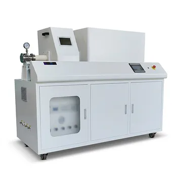
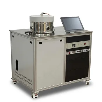
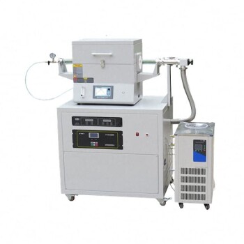
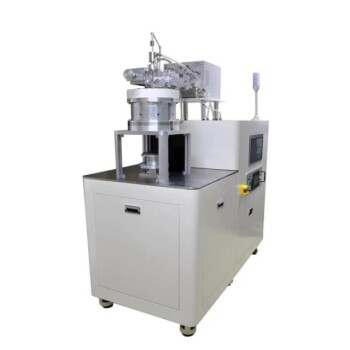
- RF PECVD System Radio Frequency Plasma-Enhanced Chemical Vapor Deposition RF PECVD
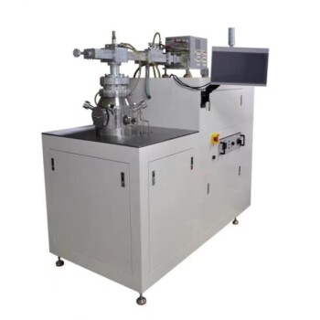
- Chemical Vapor Deposition CVD Equipment System Chamber Slide PECVD Tube Furnace with Liquid Gasifier PECVD Machine
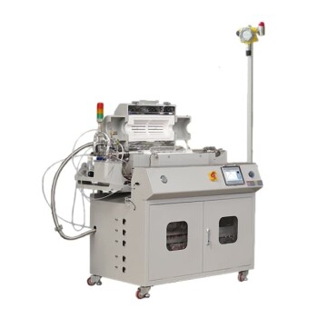
- Inclined Rotary Plasma Enhanced Chemical Vapor Deposition PECVD Equipment Tube Furnace Machine
- Inclined Rotary Plasma Enhanced Chemical Vapor Deposition PECVD Equipment Tube Furnace Machine
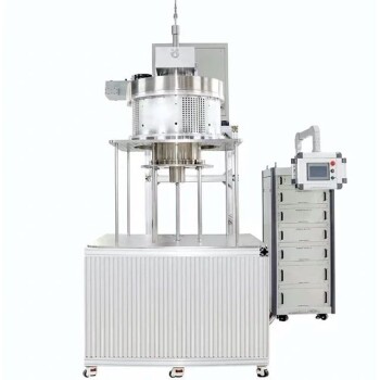
- 915MHz MPCVD Diamond Machine Microwave Plasma Chemical Vapor Deposition System Reactor
People Also Ask
- How does plasma enhance CVD? Unlock Low-Temperature, High-Quality Film Deposition
- What is plasma CVD? Unlock Low-Temperature Thin Film Deposition for Sensitive Materials
- What is plasma enhanced chemical vapour deposition process? Unlock Low-Temperature, High-Quality Thin Films
- How does Radio Frequency Enhanced Plasma Chemical Vapour Deposition (RF-PECVD) work? Learn the Core Principles
- What is plasma enhanced chemical vapour deposition PECVD used for? Enable Low-Temp Thin Films for Electronics & Solar

