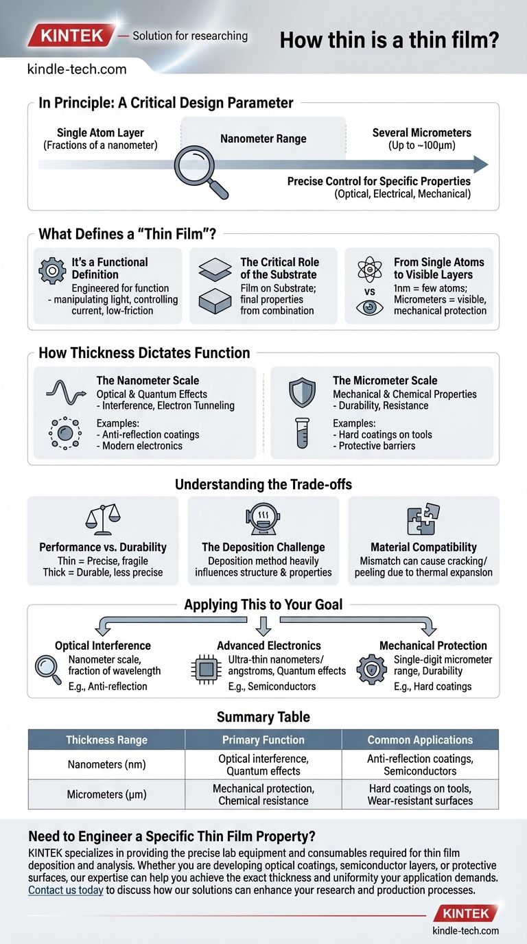
In principle, a thin film is a layer of material ranging from a single layer of atoms—fractions of a nanometer—to several micrometers in thickness. While some specialized applications can push this upper limit toward 100 micrometers, the vast majority of thin films exist in the nanometer to low-micrometer range.
A thin film's thickness is not an arbitrary measurement. It is a critical design parameter that is precisely controlled to produce specific optical, electrical, or mechanical properties that are not present in the bulk material.
What Defines a "Thin Film"?
The term "thin film" refers to more than just a physical dimension. It describes a functional state where the material's properties are dominated by surface effects and quantum phenomena rather than its bulk characteristics.
It's a Functional Definition
A layer becomes a "thin film" when its thickness is engineered to achieve a specific function. This could be manipulating light waves, controlling electrical current, or providing a durable, low-friction surface.
The Critical Role of the Substrate
Thin films are not standalone objects; they are deposited onto a base material called a substrate. The properties of the final product are a combination of the film, the substrate, and the interaction between them.
From Single Atoms to Visible Layers
To put the scale in perspective, a one-nanometer film is only a few atoms thick. Films on the micrometer scale can be thick enough to be visible and provide significant mechanical protection, like the coatings on cutting tools or eyeglasses.
How Thickness Dictates Function
The specific thickness of a film is chosen to exploit different physical phenomena. A few nanometers can make the difference between a transparent conductor and an opaque mirror.
The Nanometer Scale: Optical and Quantum Effects
At thicknesses comparable to the wavelength of light, thin films produce optical effects like interference, which is used for anti-reflection coatings on lenses. At the scale of a few nanometers, quantum effects like electron tunneling become significant, which is fundamental to modern electronics.
The Micrometer Scale: Mechanical and Chemical Properties
Thicker films, often in the 1-10 micrometer range, are used when mechanical durability or chemical resistance is the primary goal. These include hard, scratch-resistant coatings on tools and watches or protective barriers that prevent corrosion.
Understanding the Trade-offs
Choosing a film's thickness involves balancing competing requirements. The ideal solution for one property is often a compromise for another.
Performance vs. Durability
Extremely thin films are ideal for precise optical or quantum applications but can be fragile. Increasing thickness generally improves durability and scratch resistance but may interfere with the desired optical or electrical performance.
The Deposition Challenge
Creating a perfectly uniform film, especially at the nanometer scale, is a significant engineering challenge. The deposition method used to create the film heavily influences its final structure, density, and properties, often as much as the thickness itself.
Material Compatibility
The film and the substrate must be compatible. A mismatch in thermal expansion coefficients, for example, can cause the film to crack or peel off when the temperature changes, regardless of its thickness.
Applying This to Your Goal
The correct thickness is entirely dependent on the problem you are trying to solve. There is no single "best" thickness, only the right thickness for a specific application.
- If your primary focus is optical interference (e.g., anti-reflection coatings): Your thickness must be precisely controlled on the nanometer scale, often targeting a fraction of the wavelength of light.
- If your primary focus is advanced electronics (e.g., semiconductors): You will be working with ultra-thin films measured in nanometers or even angstroms to control quantum effects.
- If your primary focus is mechanical protection (e.g., hard coatings): You will typically use thicker films in the single-digit micrometer range to ensure durability and coverage.
Ultimately, the ideal thickness of a thin film is the one that precisely engineers the desired physical properties for its intended function.
Summary Table:
| Thickness Range | Primary Function | Common Applications |
|---|---|---|
| Nanometers (nm) | Optical interference, Quantum effects | Anti-reflection coatings, Semiconductors |
| Micrometers (µm) | Mechanical protection, Chemical resistance | Hard coatings on tools, Wear-resistant surfaces |
Need to Engineer a Specific Thin Film Property?
KINTEK specializes in providing the precise lab equipment and consumables required for thin film deposition and analysis. Whether you are developing optical coatings, semiconductor layers, or protective surfaces, our expertise can help you achieve the exact thickness and uniformity your application demands.
Contact us today to discuss how our solutions can enhance your research and production processes.
Visual Guide
Related Products
- RF PECVD System Radio Frequency Plasma-Enhanced Chemical Vapor Deposition RF PECVD
- Chemical Vapor Deposition CVD Equipment System Chamber Slide PECVD Tube Furnace with Liquid Gasifier PECVD Machine
- Microwave Plasma Chemical Vapor Deposition MPCVD Machine System Reactor for Lab and Diamond Growth
- Cylindrical Resonator MPCVD Machine System Reactor for Microwave Plasma Chemical Vapor Deposition and Lab Diamond Growth
- Aluminized Ceramic Evaporation Boat for Thin Film Deposition
People Also Ask
- How are PECVD and CVD different? A Guide to Choosing the Right Thin-Film Deposition Process
- What are the applications of PECVD? Essential for Semiconductors, MEMS, and Solar Cells
- What is an example of PECVD? RF-PECVD for High-Quality Thin Film Deposition
- What is plasma activated chemical vapour deposition method? A Low-Temperature Solution for Advanced Coatings
- Why is PECVD environment friendly? Understanding the Eco-Friendly Benefits of Plasma-Enhanced Coating