Knowledge How to measure thin film thickness? Choose the Right Technique for Accurate Results
Author avatar

Tech Team · Kintek Solution

Updated 6 days ago

How to measure thin film thickness? Choose the Right Technique for Accurate Results

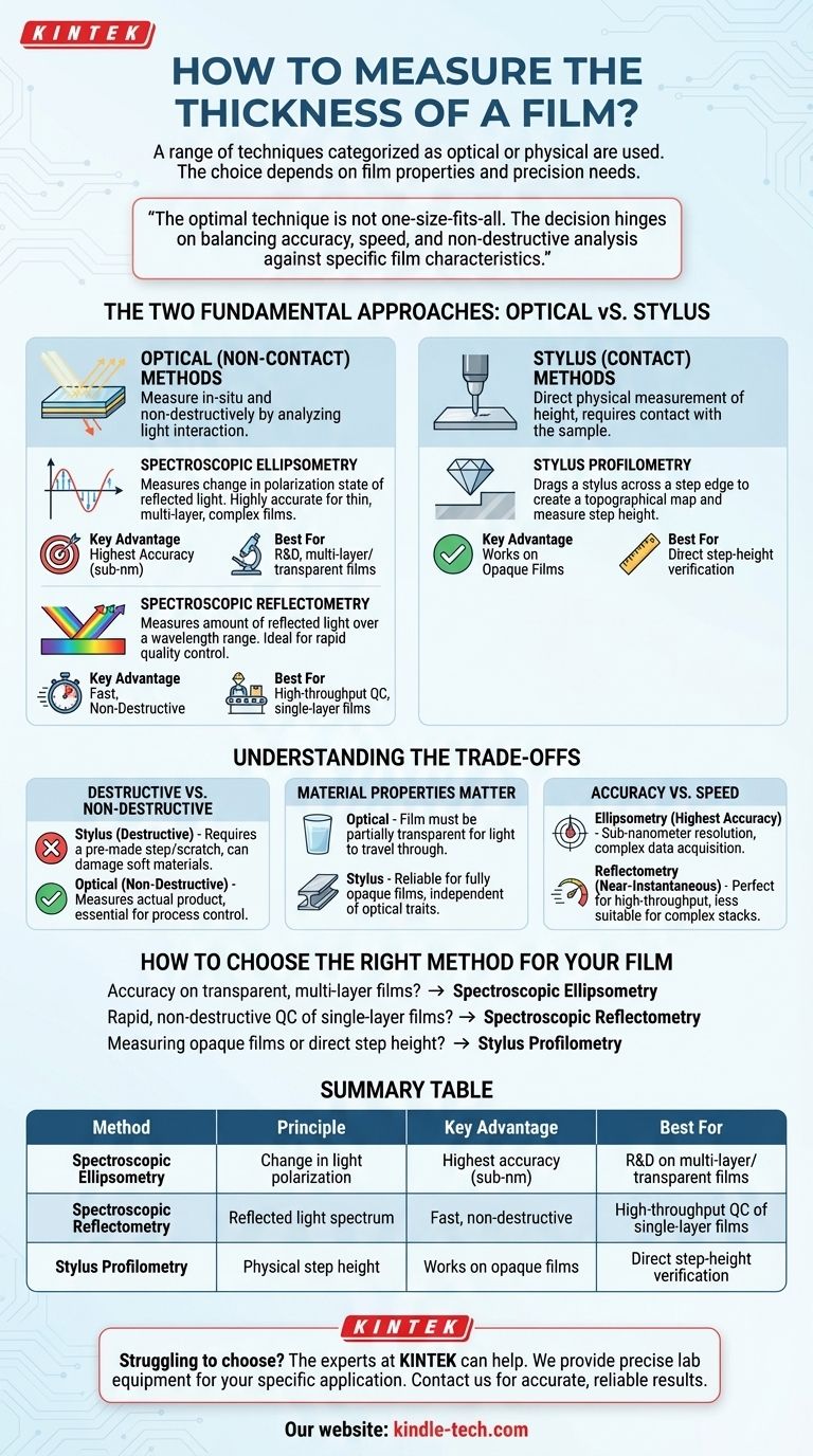
Measuring the thickness of a film is a critical process in various industries, including semiconductor manufacturing, optics, and coatings. The choice of measurement technique depends on factors such as the material properties, the thickness range, and whether the measurement is required during or after deposition. Common methods include optical techniques like ellipsometry and spectrophotometry, mechanical methods like stylus profilometry, and advanced tools like X-ray reflectivity (XRR) and electron microscopy. Each method has its advantages, such as non-destructive testing, high accuracy, or suitability for specific thickness ranges. Understanding the principles and applications of these techniques is essential for selecting the most appropriate method for a given scenario.

Key Points Explained:

How to measure thin film thickness? Choose the Right Technique for Accurate Results
  1. Optical Techniques for Thin Film Thickness Measurement

    • Ellipsometry: This method measures the change in polarization of light reflected from the film. It is highly accurate and can measure thicknesses in the nanometer range. The refractive index of the material is a critical parameter in this method.
    • Spectrophotometry: This technique analyzes the interference pattern of light reflected from the top and bottom interfaces of the film. It is suitable for measuring thicknesses between 0.3 to 60 µm and is particularly useful for microscopic sampling areas.
    • Interferometry: This method relies on the interference fringes created by a highly reflective surface. It is a non-contact technique and provides high accuracy for specific points on the film.
  2. Mechanical Methods for Thin Film Thickness Measurement

    • Stylus Profilometry: This technique involves dragging a stylus across the film surface to measure the height difference between the film and the substrate. It requires a groove or step to be present and is suitable for measuring thickness at specific points.
    • Quartz Crystal Microbalance (QCM): This method measures the mass change during film deposition by monitoring the frequency change of a quartz crystal. It is commonly used for real-time thickness monitoring during deposition.
  3. Advanced Techniques for Thin Film Thickness Measurement

    • X-ray Reflectivity (XRR): This method uses X-rays to measure the thickness and density of thin films. It is highly accurate and can measure thicknesses in the nanometer range.
    • Cross-sectional Scanning Electron Microscopy (SEM) and Transmission Electron Microscopy (TEM): These techniques provide direct imaging of the film cross-section, allowing for precise thickness measurement. However, they are destructive and require sample preparation.
  4. Factors Influencing Measurement Accuracy

    • Film Uniformity: For techniques like stylus profilometry and interferometry, film uniformity is critical as they measure thickness at specific points.
    • Refractive Index: Optical techniques like ellipsometry and spectrophotometry rely on the refractive index of the material. Different materials have different refractive indexes, which must be accurately known for precise measurements.
    • Non-Destructive Testing: Techniques like spectrophotometry and interferometry are non-contact and non-destructive, making them ideal for delicate or sensitive films.
  5. Applications and Considerations

    • Real-Time Monitoring: Techniques like QCM are used for real-time thickness monitoring during deposition, ensuring precise control over the film growth process.
    • Microscopic Sampling: Spectrophotometry is particularly useful for measuring thickness in microscopic sampling areas, making it ideal for applications in microelectronics and optics.
    • High Accuracy: Methods like XRR and ellipsometry provide high accuracy and are suitable for research and development applications where precise measurements are critical.

By understanding these key points, a purchaser or user can select the most appropriate method for measuring thin film thickness based on their specific requirements, ensuring accurate and reliable results.

Summary Table:

Method Technique Advantages Thickness Range
Optical Techniques Ellipsometry High accuracy, nanometer range 0.1 nm - 1 µm
Spectrophotometry Microscopic sampling, non-destructive 0.3 µm - 60 µm
Interferometry Non-contact, high accuracy 0.1 nm - 10 µm
Mechanical Methods Stylus Profilometry Measures specific points, requires a groove 1 nm - 100 µm
Quartz Crystal Microbalance Real-time monitoring during deposition 0.1 nm - 1 µm
Advanced Techniques X-ray Reflectivity (XRR) High accuracy, measures thickness and density 0.1 nm - 1 µm
SEM/TEM Direct imaging, precise cross-sectional measurement 0.1 nm - 1 µm

Need help selecting the right thin film thickness measurement method? Contact our experts today for tailored solutions!

Related Products

Assemble Square Lab Press Mold for Laboratory Applications

Assemble Square Lab Press Mold for Laboratory Applications

Achieve perfect sample preparation with Assemble Square Lab Press Mold. Quick disassembly eliminates sample deformation. Perfect for battery, cement, ceramics, and more. Customizable sizes available.

Lithium Battery Tab Tape for Battery Lab Applications

Lithium Battery Tab Tape for Battery Lab Applications

PI polyimide tape, generally brown, also known as gold finger tape, high temperature resistance 280 ℃, to prevent the influence of heat sealing of soft pack battery lug glue, suitable for soft pack battery tab position glue.

Cylindrical Press Mold for Lab Applications

Cylindrical Press Mold for Lab Applications

Efficiently form and test most samples with Cylindrical Press Molds in a range of sizes. Made of Japanese high-speed steel, with long service life and customizable sizes.

Graphite Vacuum Furnace High Thermal Conductivity Film Graphitization Furnace

Graphite Vacuum Furnace High Thermal Conductivity Film Graphitization Furnace

The high thermal conductivity film graphitization furnace has uniform temperature, low energy consumption and can operate continuously.

Professional Cutting Tools for Carbon Paper Cloth Diaphragm Copper Aluminum Foil and More

Professional Cutting Tools for Carbon Paper Cloth Diaphragm Copper Aluminum Foil and More

Professional tools for cutting lithium sheets, carbon paper, carbon cloth, separators, copper foil, aluminum foil, etc., with round and square shapes and different sizes of blades.

Automatic Laboratory Hydraulic Press for XRF & KBR Pellet Press

Automatic Laboratory Hydraulic Press for XRF & KBR Pellet Press

Fast and easy xrf sample pellet preparation with KinTek Automatic Lab Pellet Press. Versatile and accurate results for X-ray fluorescence analysis.

Lab Infrared Press Mold

Lab Infrared Press Mold

Easily release samples from our lab infrared press mold for accurate testing. Ideal for battery, cement, ceramics, and other sample preparation research. Customizable sizes available.

XRF & KBR steel ring lab Powder Pellet Pressing Mold for FTIR

XRF & KBR steel ring lab Powder Pellet Pressing Mold for FTIR

Produce perfect XRF samples with our steel ring lab powder pellet pressing mold. Fast tableting speed and customizable sizes for accurate molding every time.

Square Lab Press Mold for Laboratory Applications

Square Lab Press Mold for Laboratory Applications

Create uniform samples easily with Square Lab Press Mold - available in various sizes. Ideal for battery, cement, ceramics, and more. Custom sizes available.

No Demolding Lab Infrared Press Mold for Laboratory Applications

No Demolding Lab Infrared Press Mold for Laboratory Applications

Effortlessly test your samples with no demolding required using our lab infrared press mold. Enjoy high transmittance and customizable sizes for your convenience.

Manual Cold Isostatic Pressing Machine CIP Pellet Press

Manual Cold Isostatic Pressing Machine CIP Pellet Press

Lab Manual Isostatic Press is a high-efficient equipment for sample preparation widely used in material research, pharmacy, ceramics, and electronic industries. It allows for precision control of the pressing process and can work in a vacuum environment.

Custom CVD Diamond Coating for Lab Applications

Custom CVD Diamond Coating for Lab Applications

CVD Diamond Coating: Superior Thermal Conductivity, Crystal Quality, and Adhesion for Cutting Tools, Friction, and Acoustic Applications

Electric Lab Cold Isostatic Press CIP Machine for Cold Isostatic Pressing

Electric Lab Cold Isostatic Press CIP Machine for Cold Isostatic Pressing

Produce dense, uniform parts with improved mechanical properties with our Electric Lab Cold Isostatic Press. Widely used in material research, pharmacy, and electronic industries. Efficient, compact, and vacuum-compatible.

Warm Isostatic Press for Solid State Battery Research

Warm Isostatic Press for Solid State Battery Research

Discover the advanced Warm Isostatic Press (WIP) for semiconductor lamination. Ideal for MLCC, hybrid chips, and medical electronics. Enhance strength and stability with precision.

HFCVD Machine System Equipment for Drawing Die Nano-Diamond Coating

HFCVD Machine System Equipment for Drawing Die Nano-Diamond Coating

The nano-diamond composite coating drawing die uses cemented carbide (WC-Co) as the substrate, and uses the chemical vapor phase method ( CVD method for short ) to coat the conventional diamond and nano-diamond composite coating on the surface of the inner hole of the mold.

Infrared High Resistance Single Crystal Silicon Lens

Infrared High Resistance Single Crystal Silicon Lens

Silicon (Si) is widely regarded as one of the most durable mineral and optical materials for applications in the near-infrared (NIR) range, approximately 1 μm to 6 μm.

Float Soda-Lime Optical Glass for Laboratory Use

Float Soda-Lime Optical Glass for Laboratory Use

Soda-lime glass, widely favored as an insulating substrate for thin/thick film deposition, is created by floating molten glass on molten tin. This method ensures uniform thickness and exceptionally flat surfaces.

Infrared Transmission Coating Sapphire Sheet Substrate Window

Infrared Transmission Coating Sapphire Sheet Substrate Window

Crafted from sapphire, the substrate boasts unparalleled chemical, optical, and physical properties. Its remarkable resistance to thermal shocks, high temperatures, sand erosion, and water sets it apart.

High Temperature Resistant Optical Quartz Glass Sheet

High Temperature Resistant Optical Quartz Glass Sheet

Discover the power of optical glass sheets for precise light manipulation in telecommunications, astronomy, and beyond. Unlock advancements in optical technology with exceptional clarity and tailored refractive properties.

RF PECVD System Radio Frequency Plasma-Enhanced Chemical Vapor Deposition RF PECVD

RF PECVD System Radio Frequency Plasma-Enhanced Chemical Vapor Deposition RF PECVD

RF-PECVD is an acronym for "Radio Frequency Plasma-Enhanced Chemical Vapor Deposition." It deposits DLC (Diamond-like carbon film) on germanium and silicon substrates. It is utilized in the 3-12um infrared wavelength range.

Automatic Lab Cold Isostatic Press CIP Machine Cold Isostatic Pressing

Automatic Lab Cold Isostatic Press CIP Machine Cold Isostatic Pressing

Efficiently prepare samples with our Automatic Lab Cold Isostatic Press. Widely used in material research, pharmacy, and electronic industries. Provides greater flexibility and control compared to electric CIPs.

Optical Window Glass Substrate Wafer Quartz Plate JGS1 JGS2 JGS3

Optical Window Glass Substrate Wafer Quartz Plate JGS1 JGS2 JGS3

The quartz plate is a transparent, durable, and versatile component widely used in various industries. Made from high-purity quartz crystal, it exhibits excellent thermal and chemical resistance.

Optical Window Glass Substrate Wafer Barium Fluoride BaF2 Substrate Window

Optical Window Glass Substrate Wafer Barium Fluoride BaF2 Substrate Window

BaF2 is the fastest scintillator, sought-after for its exceptional properties. Its windows and plates are valuable for VUV and infrared spectroscopy.

Zinc Selenide ZnSe Optical Window Glass Substrate Wafer and Lens

Zinc Selenide ZnSe Optical Window Glass Substrate Wafer and Lens

Zinc selenide is formed by synthesizing zinc vapor with H2Se gas, resulting in sheet-like deposits on graphite susceptors.

Optical Window Glass Substrate Wafer Sheets Zinc Sulfide ZnS Window

Optical Window Glass Substrate Wafer Sheets Zinc Sulfide ZnS Window

Optics Zinc Sulphide (ZnS) Windows have an excellent IR transmission range between 8-14 microns.Excellent mechanical strength and chemical inertness for harsh environments (harder than ZnSe Windows)

400-700nm Wavelength Anti Reflective AR Coating Glass

400-700nm Wavelength Anti Reflective AR Coating Glass

AR coatings are applied on optical surfaces to reduce reflection. They can be a single layer or multiple layers that are designed to minimize reflected light through destructive interference.

Optical Ultra-Clear Glass Sheet for Laboratory K9 B270 BK7

Optical Ultra-Clear Glass Sheet for Laboratory K9 B270 BK7

Optical glass, while sharing many characteristics with other types of glass, is manufactured using specific chemicals that enhance properties crucial for optics applications.

Optical Window Glass Substrate Wafer CaF2 Substrate Window Lens

Optical Window Glass Substrate Wafer CaF2 Substrate Window Lens

A CaF2 window is an optical window made of crystalline calcium fluoride. These windows are versatile, environmentally stable and resistant to laser damage, and they exhibit a high, stable transmission from 200 nm to about 7 μm.

MgF2 Magnesium Fluoride Crystal Substrate Window for Optical Applications

MgF2 Magnesium Fluoride Crystal Substrate Window for Optical Applications

Magnesium fluoride (MgF2) is a tetragonal crystal that exhibits anisotropy, making it imperative to treat it as a single crystal when engaging in precision imaging and signal transmission.

Electrode Polishing Material for Electrochemical Experiments

Electrode Polishing Material for Electrochemical Experiments

Looking for a way to polish your electrodes for electrochemical experiments? Our polishing materials are here to help! Follow our easy instructions for best results.


Leave Your Message