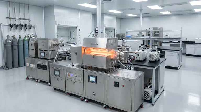
At its core, Chemical Vapor Deposition (CVD) is an exceptionally versatile and precise manufacturing process. Its primary advantages stem from its unique method of building materials atom by atom from chemical precursors, allowing for the creation of high-purity, uniform, and durable thin films on a vast range of substrates, including those with complex shapes.
The fundamental strength of CVD is its reliance on controlled chemical reactions rather than physical line-of-sight application. This allows it to produce superior, highly uniform coatings that can penetrate intricate geometries, making it a foundational technology in industries from semiconductors to advanced materials.
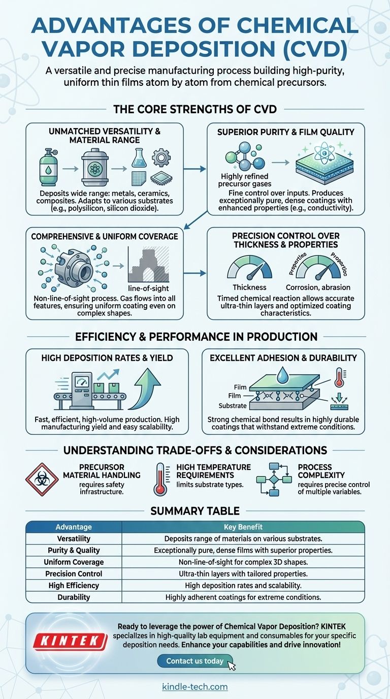
The Core Strengths of Chemical Vapor Deposition
The advantages of CVD are not isolated benefits but interconnected strengths that arise directly from its gas-phase chemical process. Understanding these principles is key to leveraging the technology effectively.
Unmatched Versatility and Material Range
CVD is not limited to a specific class of materials. Because the process is driven by the chemistry of the precursor gases, it can be adapted to deposit everything from metals and ceramics to specialized composites.
This allows it to be used on a wide array of substrates, including glass, metals, and ceramics. Materials like polysilicon, critical for the solar industry, and silicon dioxide, a cornerstone of microelectronics, are commonly produced using CVD.
Superior Purity and Film Quality
The process allows for exceptionally fine control over the inputs. By using highly refined precursor gases, CVD can generate films and coatings that are incredibly pure and dense.
This purity translates to enhanced material properties, such as greater electrical and thermal conductivity and better compatibility when mixed with other materials. The resulting surfaces are also exceptionally smooth.
Comprehensive and Uniform Coverage
A defining feature of CVD is that it is a non-line-of-sight process. The precursor gases flow and diffuse into every crevice and feature of a component before reacting to form the solid film.
This ensures a completely uniform coating, even on components with complex, three-dimensional shapes. This capability is difficult or impossible to achieve with line-of-sight methods, which can create "shadows" or areas of thin coverage.
Precision Control Over Thickness and Properties
Because the film is built up through a timed chemical reaction, engineers have full control over the process. This allows for the creation of ultra-thin layers with remarkable accuracy and thickness control.
This precision is essential for applications like electrical circuits and semiconductors. Furthermore, the gas chemistry can be optimized to produce coatings with specific characteristics, such as enhanced corrosion resistance or abrasion resistance.
Efficiency and Performance in Production
Beyond its technical capabilities, CVD offers significant practical advantages for manufacturing and high-performance applications.
High Deposition Rates and Yield
CVD systems are generally fast and efficient, capable of depositing material at high rates. This makes them well-suited for high-volume production environments.
The process is also known for its high manufacturing yield and relative simplicity in scaling up from laboratory development to full-scale industrial production.
Excellent Adhesion and Durability
The chemical bond formed between the deposited film and the substrate during the CVD process results in commendable adhesion.
This creates highly durable coatings that can withstand high-stress environments, extreme temperatures, and significant temperature variations without delamination or failure.
Understanding the Trade-offs and Considerations
While powerful, CVD is not a universal solution. An objective assessment requires acknowledging its operational complexities and requirements.
Precursor Material Handling
The precursor gases used in CVD can be expensive, toxic, corrosive, or flammable. This necessitates significant investment in safety infrastructure, handling protocols, and supply chain management.
High Temperature Requirements
Many, though not all, CVD processes require very high temperatures to initiate the necessary chemical reactions. This can limit the types of substrate materials that can be coated, as some may be damaged or deformed by the heat.
Process Complexity
Achieving the high-quality results CVD is known for requires precise control over multiple variables simultaneously. Factors like temperature, pressure, gas flow rates, and reactor geometry must be carefully optimized, which can make process development a complex undertaking.
Making the Right Choice for Your Goal
Selecting a deposition technology depends entirely on your end goal. CVD excels in specific scenarios where its unique advantages provide a clear path to success.
- If your primary focus is advanced electronics or semiconductors: CVD's ability to create ultra-thin, exceptionally pure films with precise, uniform thickness control is its most critical advantage.
- If your primary focus is durable industrial coatings: The key benefit is CVD's capacity to form dense, highly adherent layers with tailored wear, corrosion, and heat resistance, even on complex parts.
- If your primary focus is high-volume, high-purity material production: The combination of high deposition rates, scalability, and consistent quality makes CVD an efficient and reliable choice.
Ultimately, Chemical Vapor Deposition empowers engineers to build superior materials from the ground up, making it an indispensable tool for modern innovation.
Summary Table:
| Advantage | Key Benefit |
|---|---|
| Versatility | Deposits a wide range of materials (metals, ceramics) on various substrates. |
| Purity & Quality | Produces exceptionally pure, dense films with superior material properties. |
| Uniform Coverage | Non-line-of-sight process ensures even coating on complex 3D shapes. |
| Precision Control | Enables ultra-thin layers with accurate thickness and tailored properties. |
| High Efficiency | High deposition rates and scalability for volume production. |
| Durability | Creates highly adherent coatings that withstand extreme conditions. |
Ready to leverage the power of Chemical Vapor Deposition in your research or production?
KINTEK specializes in providing high-quality lab equipment and consumables to meet your specific deposition needs. Whether you are developing advanced semiconductors, durable industrial coatings, or high-purity materials, our expertise and solutions can help you achieve superior results with efficiency and precision.
Contact us today to discuss how our CVD solutions can enhance your laboratory's capabilities and drive your innovations forward!
Visual Guide
Related Products
- Chemical Vapor Deposition CVD Equipment System Chamber Slide PECVD Tube Furnace with Liquid Gasifier PECVD Machine
- Microwave Plasma Chemical Vapor Deposition MPCVD Machine System Reactor for Lab and Diamond Growth
- 915MHz MPCVD Diamond Machine Microwave Plasma Chemical Vapor Deposition System Reactor
- Customer Made Versatile CVD Tube Furnace Chemical Vapor Deposition Chamber System Equipment
- RF PECVD System Radio Frequency Plasma-Enhanced Chemical Vapor Deposition RF PECVD
People Also Ask
- What are the processes of vapor phase deposition? Understand CVD vs. PVD for Superior Thin Films
- What types of substrates are used in CVD to facilitate graphene films? Optimize Graphene Growth with the Right Catalyst
- What is plasma enhanced chemical vapor deposition PECVD equipment? A Guide to Low-Temperature Thin Film Deposition
- Why is Chemical Vapor Deposition (CVD) equipment uniquely suited for constructing hierarchical superhydrophobic structures?
- How are carbon nanotubes grown? Master Scalable Production with Chemical Vapor Deposition


