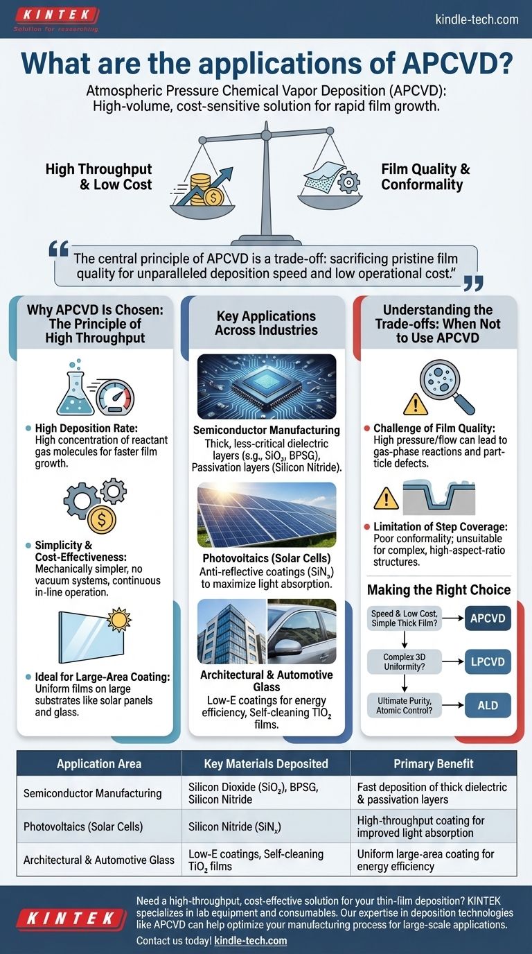
At its core, Atmospheric Pressure Chemical Vapor Deposition (APCVD) is used for high-volume, cost-sensitive applications where rapid film growth is more critical than perfect structural quality. Its primary applications are found in semiconductor manufacturing for dielectric layers, in photovoltaics for anti-reflective coatings, and in coating large sheets of architectural glass.
The central principle of APCVD is a trade-off: it sacrifices the pristine film quality and conformality of low-pressure vacuum systems for unparalleled deposition speed and low operational cost, making it the workhorse for specific, less-critical thin-film applications.
Why APCVD Is Chosen: The Principle of High Throughput
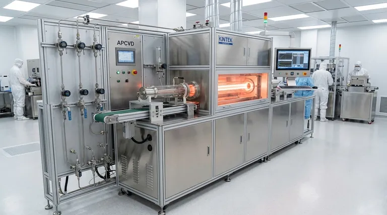
The decision to use APCVD is almost always driven by economics and scale. The process is defined by its operation at standard atmospheric pressure, which eliminates the need for expensive and slow vacuum systems.
The Advantage of Atmospheric Pressure
Operating at atmospheric pressure means a high concentration of reactant gas molecules is available at the substrate surface.
This high concentration leads to a very high deposition rate, allowing films to be grown much faster than in low-pressure or vacuum-based systems.
Simplicity and Cost-Effectiveness
APCVD systems are mechanically simpler and therefore less expensive to build and maintain than their vacuum-based counterparts like LPCVD or PECVD.
They are often designed as continuous, in-line systems where substrates move on a conveyor belt, enabling massive throughput ideal for large-scale manufacturing.
Ideal for Large-Area Coating
The continuous nature of APCVD makes it exceptionally well-suited for depositing uniform films over very large surface areas.
This capability is essential for industries producing items like solar panels or large panes of architectural glass, where batch processing in a vacuum chamber would be impractical.
Key Applications Across Industries
APCVD's unique characteristics make it the preferred choice for several high-volume manufacturing processes where its strengths align perfectly with industry needs.
Semiconductor Manufacturing
In fabricating integrated circuits, APCVD is used for thick, less-critical dielectric layers.
Its most common use is for depositing doped and undoped silicon dioxide (SiO₂). This includes films like Borophosphosilicate glass (BPSG), which is used as a pre-metal dielectric (PMD) layer that can be smoothed or "reflowed" at high temperatures to create a planar surface for subsequent metal layers. It is also used for shallow trench isolation (STI).
APCVD can also be used for final passivation layers, such as silicon nitride, that protect the finished chip from moisture and mechanical damage.
Photovoltaics (Solar Cells)
The solar industry requires coating very large silicon wafers quickly and cheaply. APCVD is the dominant method for this.
It is primarily used to deposit anti-reflective coatings, typically silicon nitride (SiNₓ), on the surface of solar cells. This layer maximizes the amount of light absorbed by the cell, directly increasing its efficiency.
Architectural and Automotive Glass
For the construction and automotive industries, APCVD is used to apply functional coatings to large sheets of glass.
A major application is the deposition of low-emissivity (Low-E) coatings. These films reflect infrared radiation, helping to keep heat inside during the winter and outside during the summer, improving energy efficiency. Self-cleaning coatings, often based on titanium dioxide (TiO₂), are another common application.
Understanding the Trade-offs: When Not to Use APCVD
While powerful, APCVD is not a universal solution. Its weaknesses are the direct consequence of the same atmospheric conditions that provide its strengths.
The Challenge of Film Quality
The high pressure and gas flow rates can lead to unwanted chemical reactions in the gas phase before the precursors reach the substrate.
This can form tiny particles that land on the film, creating defects and reducing the overall purity and electronic quality of the layer.
The Limitation of Step Coverage
APCVD exhibits poor step coverage, or conformality. The film it deposits is not uniform over complex, three-dimensional surface topography.
Because reactant transport is limited by diffusion through a thick boundary layer, the film will be much thicker on top surfaces than on the sidewalls of a trench or via. This makes it unsuitable for coating the intricate, high-aspect-ratio structures found in modern, high-density microchips.
Making the Right Choice for Your Process
Selecting a deposition technology requires matching the process capabilities to the specific requirements of the film and the economic realities of the product.
- If your primary focus is speed and low cost for a relatively simple, thick film: APCVD is the optimal choice, especially for dielectrics, passivation layers, and large-area coatings.
- If your primary focus is coating complex 3D structures uniformly: You must use a process with better conformality, such as Low-Pressure CVD (LPCVD).
- If your primary focus is ultimate purity, atomic-level thickness control, and perfect conformality: The necessary technology is Atomic Layer Deposition (ALD).
Ultimately, choosing APCVD is a strategic decision to prioritize manufacturing throughput and cost for applications that can tolerate its inherent limitations in film quality and conformality.
Summary Table:
| Application Area | Key Materials Deposited | Primary Benefit |
|---|---|---|
| Semiconductor Manufacturing | Silicon Dioxide (SiO₂), Borophosphosilicate Glass (BPSG), Silicon Nitride | Fast deposition of thick dielectric & passivation layers |
| Photovoltaics (Solar Cells) | Silicon Nitride (SiNₓ) anti-reflective coatings | High-throughput coating for improved light absorption |
| Architectural & Automotive Glass | Low-E coatings, Self-cleaning TiO₂ films | Uniform large-area coating for energy efficiency |
Need a high-throughput, cost-effective solution for your thin-film deposition? KINTEK specializes in lab equipment and consumables, serving laboratory needs. Our expertise in deposition technologies like APCVD can help you optimize your manufacturing process for large-scale applications. Contact us today to discuss how our solutions can enhance your production efficiency and reduce costs!
Visual Guide
Related Products
- Inclined Rotary Plasma Enhanced Chemical Vapor Deposition PECVD Equipment Tube Furnace Machine
- Multi Heating Zones CVD Tube Furnace Machine Chemical Vapor Deposition Chamber System Equipment
- Chemical Vapor Deposition CVD Equipment System Chamber Slide PECVD Tube Furnace with Liquid Gasifier PECVD Machine
- Inclined Rotary Plasma Enhanced Chemical Vapor Deposition PECVD Equipment Tube Furnace Machine
- RF PECVD System Radio Frequency Plasma-Enhanced Chemical Vapor Deposition RF PECVD
People Also Ask
- What is the necessity of depositing a silicon nitride (SiNx) thin film using PECVD? Optimize QSSPC Lifetime Measurement
- What are the advantages of plasma enhanced chemical vapor deposition? Enable Low-Temperature, High-Quality Film Deposition
- What are the benefits of plasma enhanced CVD? Achieve High-Quality, Low-Temperature Film Deposition
- Why is a PECVD system required for vertical graphene synthesis? Master Directional Control for 3D Nanostructures
- What is plasma enhanced chemical vapour deposition PECVD used for? Enable Low-Temp Thin Films for Electronics & Solar


