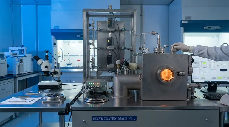
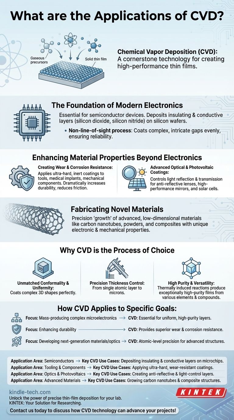
At its core, Chemical Vapor Deposition (CVD) is a cornerstone technology for creating high-performance thin films. It is most prominently used in the semiconductor industry to build microchips, but its applications also extend to creating protective coatings for tools, advanced optical components, and even solar cells. The process involves using gaseous chemical precursors to deposit a solid material, layer by atomic layer, onto a substrate.
The true value of CVD lies in its unparalleled control over material deposition at the atomic level. This precision allows it to create perfectly uniform, high-purity layers on complex surfaces, a capability that is fundamental to modern electronics and materials science.
The Foundation of Modern Electronics
The most significant application of CVD is in the fabrication of semiconductor devices. The process is not just a part of chipmaking; it is an essential step that makes modern microelectronics possible.
Building the Microchip Layer by Layer
CVD is used to deposit critical insulating (dielectric) and conductive thin films onto silicon wafers. Materials like silicon dioxide and silicon nitride are deposited to electrically isolate the billions of transistors on a single chip, preventing short circuits.
Filling Intricate Gaps
As microchips become more complex, their physical structures contain microscopic trenches and gaps. CVD is a "non-line-of-sight" process, meaning the chemical vapor can reach and coat every surface evenly, no matter how intricate. This ensures complete, uniform coverage, which is critical for device reliability.
Enhancing Material Properties Beyond Electronics
While central to semiconductors, the unique capabilities of CVD are leveraged across numerous other high-tech industries to grant materials properties they do not naturally possess.
Creating Wear and Corrosion Resistance
CVD is used to apply ultra-hard, chemically inert coatings to industrial tools, medical implants, and mechanical components. These coatings dramatically increase durability, reduce friction, and protect the underlying material from harsh environments.
Advanced Optical and Photovoltaic Coatings
In the optical and opto-electrical industries, CVD is used to deposit thin films that control the reflection and transmission of light. This is crucial for creating anti-reflective lenses, high-performance mirrors, and the functional layers within solar panels (photovoltaics).
Fabricating Novel Materials
The precision of CVD allows for the "growth" of advanced, low-dimensional materials. It is a primary method for producing structures like carbon nanotubes, powders, and composite materials, which have unique and valuable electronic and mechanical properties.
Why CVD is the Process of Choice
Other deposition methods exist, but CVD is chosen when certain characteristics are non-negotiable. Its advantages are directly tied to the fundamental nature of the process.
Unmatched Conformality and Uniformity
Because CVD uses a gas to deposit material, it coats all exposed surfaces with a perfectly even layer. This ability to create a conformal coating on complex, three-dimensional shapes is its most powerful advantage and is extremely difficult to achieve with other processes.
Precision Thickness Control
The process allows for exquisite control over the thickness of the deposited film. Engineers can specify a layer ranging from a single sheet of atoms to several microns thick, enabling the precise tuning of a component's electrical, optical, or mechanical properties.
High Purity and Versatility
The thermally induced chemical reactions inherent to CVD produce films of exceptionally high purity. Furthermore, the process is incredibly versatile and can be adapted to deposit a wide range of elements and compounds, from metals to ceramics.
How CVD Applies to Specific Goals
The decision to use CVD is driven by the desired outcome for the final product.
- If your primary focus is mass-producing complex microelectronics: CVD is the essential standard for depositing the uniform, high-purity insulating and conductive layers that make modern chips functional.
- If your primary focus is enhancing the durability of mechanical parts: CVD provides superior wear and corrosion resistance by coating components with hard, inert films that extend their operational life.
- If your primary focus is developing next-generation materials or optics: CVD offers the atomic-level precision required to grow advanced structures like carbon nanotubes or create specialized optical coatings.
Ultimately, CVD is the enabling process for any application that demands absolute control over the structure and properties of a material's surface.
Summary Table:
| Application Area | Key CVD Use Cases |
|---|---|
| Semiconductors | Depositing insulating & conductive layers on microchips |
| Tooling & Components | Applying ultra-hard, wear-resistant coatings |
| Optics & Photovoltaics | Creating anti-reflective & light-control layers |
| Advanced Materials | Growing carbon nanotubes & composite structures |
Unlock the power of precise thin-film deposition for your lab.
KINTEK specializes in providing high-performance CVD equipment and consumables tailored to your research and production needs. Whether you're developing next-generation semiconductors, durable coatings, or advanced optical components, our solutions deliver the uniformity, purity, and control your work demands.
Contact us today to discuss how CVD technology can advance your projects!
Visual Guide
Related Products
- Chemical Vapor Deposition CVD Equipment System Chamber Slide PECVD Tube Furnace with Liquid Gasifier PECVD Machine
- Customer Made Versatile CVD Tube Furnace Chemical Vapor Deposition Chamber System Equipment
- HFCVD Machine System Equipment for Drawing Die Nano-Diamond Coating
- Multi Heating Zones CVD Tube Furnace Machine Chemical Vapor Deposition Chamber System Equipment
- CVD Diamond Dressing Tools for Precision Applications
People Also Ask
- What types of substrates are used in CVD to facilitate graphene films? Optimize Graphene Growth with the Right Catalyst
- What is the chemical vapor deposition growth process? Build Superior Thin Films from the Atom Up
- What are the processes of vapor phase deposition? Understand CVD vs. PVD for Superior Thin Films
- How are carbon nanotubes grown? Master Scalable Production with Chemical Vapor Deposition
- Why is Chemical Vapor Deposition (CVD) equipment uniquely suited for constructing hierarchical superhydrophobic structures?


