In short, DC sputtering is a foundational technology for depositing thin metallic and conductive films across numerous high-tech industries. Its applications range from creating the reflective metal layers on CDs and DVDs to producing the anti-reflective coatings on optical lenses and manufacturing the metallic interconnects on semiconductor chips.
The defining characteristic of DC sputtering is its reliance on an electrically conductive target. This makes it an exceptionally cost-effective and controllable method for depositing metals and other conductive thin films, but it fundamentally restricts its use to materials that can sustain a direct electrical current.
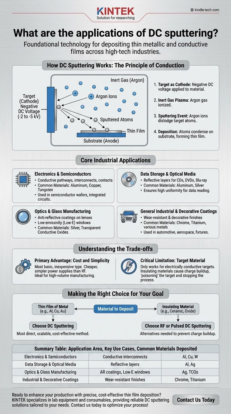
How DC Sputtering Works: The Principle of Conduction
To understand its applications, you must first understand its core mechanism. DC sputtering is a physical vapor deposition (PVD) process that functions like atomic-scale sandblasting, driven by a simple electrical circuit.
The Target as a Cathode
The process begins by applying a strong, negative direct current (DC) voltage, typically -2 to -5 kV, to the material you want to deposit. This material, known as the target, acts as the cathode in the circuit.
The Role of Inert Gas
The entire process occurs in a vacuum chamber filled with a small amount of an inert gas, almost always argon. The DC voltage energizes the chamber, stripping electrons from the argon atoms and creating a glowing plasma of positively charged argon ions.
The Sputtering Event
These positive argon ions are powerfully attracted to the negatively charged target. They accelerate and collide with the target's surface with significant force, physically knocking off, or "sputtering," individual atoms of the target material.
Deposition on the Substrate
These ejected atoms travel through the vacuum chamber and condense on a nearby object, known as the substrate. Over time, these atoms build up to form a uniform, high-quality thin film.
Core Industrial Applications
The requirement for an electrically conductive target makes DC sputtering the ideal choice for a specific, yet vast, range of industrial uses.
Electronics and Semiconductors
This is a primary application area. DC sputtering is used to deposit the thin layers of metal (like aluminum, copper, or tungsten) that form the conductive pathways, interconnects, and contacts on semiconductor wafers and integrated circuits.
Data Storage and Optical Media
The shiny, reflective layers on CDs, DVDs, and Blu-ray discs are created using DC sputtering to deposit a thin film of aluminum or another reflective metal. This process ensures high uniformity and reflectivity, which is critical for the laser to read the data.
Optics and Glass Manufacturing
DC sputtering is used to apply anti-reflective coatings on camera lenses, eyeglasses, and other optical equipment. It is also the core technology behind low-emissivity (Low-E) windows, where a microscopically thin, transparent layer of metal (like silver) is sputtered onto glass to reflect thermal energy and improve insulation.
General Industrial and Decorative Coatings
The technology is widely used to apply wear-resistant or decorative coatings on a variety of products. This includes everything from automotive parts and aerospace components to household fixtures, providing both durability and a desired metallic finish.
Understanding the Trade-offs
No technology is universal. The choice to use DC sputtering is dictated by its distinct advantages and one critical limitation.
The Primary Advantage: Cost and Simplicity
DC sputtering is the most basic and inexpensive type of sputtering. The required DC power supplies are significantly cheaper and simpler than the radio-frequency (RF) systems needed for other materials. This makes it exceptionally attractive for high-volume, cost-sensitive industrial manufacturing.
The Critical Limitation: Target Material
Standard DC sputtering only works for electrically conductive targets. If you attempt to use an insulating (dielectric) material like a ceramic or oxide, positive charge from the argon ions rapidly builds up on the target's surface. This "poisons" the target, neutralizing the negative voltage and stopping the sputtering process entirely.
When to Use Alternatives
For depositing insulating materials, technicians must use other methods. RF (Radio Frequency) sputtering alternates the voltage at high frequency, preventing charge buildup. Pulsed DC sputtering accomplishes a similar goal by rapidly switching the DC voltage on and off.
Making the Right Choice for Your Goal
Selecting the right deposition technique comes down to the material you intend to use.
- If your primary focus is depositing a thin film of metal (like aluminum, copper, or gold): DC sputtering is almost always the most direct, scalable, and cost-effective method.
- If your primary focus is high-volume manufacturing of conductive coatings: The low cost and process stability of DC sputtering make it the superior choice for industrial production.
- If your primary focus is depositing an insulating material (like a ceramic or oxide): You must look beyond standard DC sputtering to alternatives like RF or Pulsed DC sputtering to avoid charge buildup on the target.
Understanding this fundamental constraint of electrical conductivity is the key to leveraging DC sputtering effectively in your projects.
Summary Table:
| Application Area | Key Use Cases | Common Materials Deposited |
|---|---|---|
| Electronics & Semiconductors | Conductive interconnects, contacts | Aluminum, Copper, Tungsten |
| Data Storage & Optical Media | Reflective layers for CDs, DVDs | Aluminum, Silver |
| Optics & Glass Manufacturing | Anti-reflective coatings, Low-E windows | Silver, Transparent conductive oxides |
| Industrial & Decorative Coatings | Wear-resistant, decorative finishes | Various metals (e.g., Chrome, Titanium) |
Ready to enhance your production with precise, cost-effective thin film deposition? KINTEK specializes in lab equipment and consumables, providing reliable DC sputtering solutions tailored to your laboratory's needs. Whether you're in semiconductor manufacturing, optics, or R&D, our expertise ensures high-quality conductive coatings with superior uniformity and adhesion. Contact us today to discuss how our DC sputtering systems can optimize your process and drive innovation!
Visual Guide
Related Products
People Also Ask
- Under what conditions should a carbon fiber brush be replaced? Identify Critical Failure to Ensure Performance
- What checks should be performed on a carbon fiber brush before use? Ensure Reliability in Your Lab Processes
- What does the regular maintenance inspection of a carbon fiber brush entail? Ensure Peak Performance and Longevity
- How should a carbon fiber brush be pre-treated to enhance microbial attachment? Optimize Your Bioelectrochemical System
- Why is it important to prevent mechanical damage to a carbon fiber brush? Ensure Peak Performance & Longevity