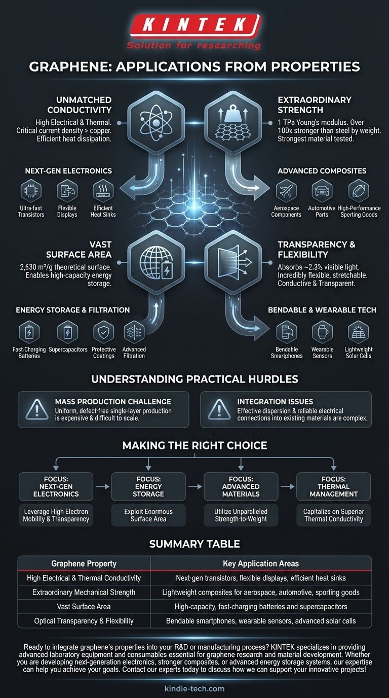
At its core, graphene's applications stem from its status as the strongest, thinnest, and most conductive material ever isolated. Its unique combination of properties, including extreme mechanical strength, high electrical and thermal conductivity, and optical transparency, enables its use in next-generation electronics, advanced composite materials, and high-capacity energy storage systems.
The true potential of graphene lies not in a single superlative property, but in the unprecedented combination of several. It is simultaneously strong, lightweight, flexible, transparent, and highly conductive, a profile that unlocks applications previously confined to science fiction.
How Graphene's Properties Drive Its Applications
Graphene is a single, two-dimensional layer of carbon atoms arranged in a hexagonal lattice. This simple structure gives rise to a set of extraordinary characteristics that directly translate into groundbreaking real-world uses.
Unmatched Electrical and Thermal Conductivity
Graphene boasts exceptionally high electron mobility and is one of the most thermally conductive materials known. Its critical current density—the amount of electrical current it can withstand—is orders of magnitude higher than copper.
These properties make it ideal for next-generation electronics. Applications include ultra-fast transistors, transparent conductive films for touch screens and flexible displays, and highly efficient heat sinks for dissipating waste heat in microprocessors.
Extraordinary Mechanical Strength
With a Young's modulus of around 1 TerPascal (TPa), graphene is over 100 times stronger than steel by weight. It is the strongest material ever tested.
This strength-to-weight ratio is being harnessed to create ultra-strong, lightweight composite materials. By mixing small amounts of graphene into polymers, plastics, or metals, manufacturers can significantly enhance strength and durability for use in aerospace, automotive components, and high-performance sporting goods.
Vast Surface Area and Chemical Inertness
Theoretically, graphene has a specific surface area of 2,630 square meters per gram. This means a single gram could cover nearly half a football field.
This enormous surface area is critical for energy storage applications. It allows for the creation of supercapacitors and batteries that can store significantly more energy and charge much faster than conventional technologies. Its inertness also makes it a promising material for protective coatings and advanced filtration membranes.
Optical Transparency and Flexibility
Despite its strength, a single layer of graphene is almost completely transparent, absorbing only about 2.3% of visible light. It is also incredibly flexible and can be stretched without breaking.
This unique combination of being conductive, transparent, and flexible is revolutionary. It opens the door to bendable smartphones, wearable electronic sensors integrated into clothing, and more efficient, lightweight solar cells that can be applied to any surface.
Understanding the Practical Hurdles
While graphene's properties are remarkable, its widespread adoption faces significant real-world challenges. Understanding these limitations is crucial for any practical assessment.
The Challenge of Mass Production
Producing large, uniform, and defect-free sheets of single-layer graphene remains a major technical and economic hurdle. Many current production methods are expensive and do not scale easily for industrial use.
Much of the "graphene" used in consumer products today is actually graphene nanoplatelets or graphene oxide, which do not exhibit the same perfect properties as a pristine single layer.
Integration and Compatibility
Effectively integrating graphene into existing materials and manufacturing processes is a complex engineering problem. Ensuring that the graphene disperses properly within a composite to impart its strength, or making a reliable electrical connection to it in a circuit, requires specialized techniques that are still being perfected.
Making the Right Choice for Your Goal
To leverage graphene effectively, you must align its specific properties with your primary objective.
- If your primary focus is next-generation electronics: Leverage its high electron mobility and transparency for faster components and flexible displays.
- If your primary focus is energy storage: Exploit its enormous surface area to design high-capacity, fast-charging batteries and supercapacitors.
- If your primary focus is advanced materials: Utilize its unparalleled strength-to-weight ratio to engineer stronger, lighter, and more durable composites.
- If your primary focus is thermal management: Capitalize on its superior thermal conductivity to create highly efficient heat spreaders and cooling solutions.
Understanding how to map these fundamental properties to specific applications is the key to unlocking graphene's transformative potential.
Summary Table:
| Graphene Property | Key Application Areas |
|---|---|
| High Electrical & Thermal Conductivity | Next-generation transistors, flexible displays, efficient heat sinks |
| Extraordinary Mechanical Strength | Lightweight composites for aerospace, automotive, and sporting goods |
| Vast Surface Area | High-capacity, fast-charging batteries and supercapacitors |
| Optical Transparency & Flexibility | Bendable smartphones, wearable sensors, and advanced solar cells |
Ready to integrate graphene's properties into your R&D or manufacturing process? KINTEK specializes in providing advanced laboratory equipment and consumables essential for graphene research and material development. Our solutions support the precise synthesis, analysis, and integration of nanomaterials like graphene. Whether you are developing next-generation electronics, stronger composites, or advanced energy storage systems, our expertise can help you achieve your goals. Contact our experts today to discuss how we can support your innovative projects!
Visual Guide
Related Products
- Graphite Vacuum Furnace High Thermal Conductivity Film Graphitization Furnace
- Graphite Disc Rod and Sheet Electrode Electrochemical Graphite Electrode
- Ultra-High Temperature Graphite Vacuum Graphitization Furnace
- Vertical High Temperature Graphite Vacuum Graphitization Furnace
- High Purity Pure Graphite Crucible for Evaporation
People Also Ask
- What is the temperature of a graphite furnace? Achieve Extreme Heat Up to 3000°C
- What are the advantages and disadvantages of graphite furnace? Unlock Extreme Heat Performance
- What is the use of graphite furnace? Achieve Extreme-Temperature Processing for Advanced Materials
- What are the interferences of graphite furnace? Overcome Matrix & Spectral Issues for Accurate GFAAS
- What are the disadvantages of graphite furnace? Key Limitations and Operational Costs