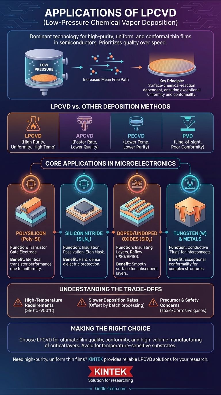
At its core, Low-Pressure Chemical Vapor Deposition (LPCVD) is the dominant technology for depositing extremely high-purity, uniform, and conformal thin films in the semiconductor industry. Its primary applications include creating polysilicon for transistor gates, silicon nitride for insulation and masking, and various doped and undoped oxides that form the foundational layers of modern integrated circuits.
While other deposition methods exist, LPCVD is selected when the quality, purity, and uniformity of the film are more critical than the deposition speed. It excels at coating complex, three-dimensional microstructures evenly, a requirement that is non-negotiable in high-performance electronics.
The Principle Behind LPCVD's Power
To understand its applications, you must first understand why the "low pressure" is so significant. LPCVD systems operate in a vacuum, which fundamentally changes how gas molecules behave.
The Role of Low Pressure
By reducing the system pressure, the mean free path—the average distance a gas molecule travels before colliding with another—is significantly increased.
This has a direct and powerful consequence: the deposition process becomes less dependent on gas flow dynamics and more on surface chemical reactions. The result is a film that is exceptionally uniform across the wafer and highly conformal, meaning it coats vertical and horizontal surfaces with near-equal thickness.
LPCVD vs. Other Deposition Methods
LPCVD does not exist in a vacuum, technologically speaking. It is chosen for specific reasons over other methods:
- Atmospheric Pressure CVD (APCVD): Faster deposition rates but produces lower-quality films with poor conformity.
- Plasma-Enhanced CVD (PECVD): Allows for deposition at much lower temperatures but can result in lower film purity and density due to hydrogen incorporation.
- Physical Vapor Deposition (PVD): A "line-of-sight" technique that is excellent for depositing metals but struggles to conformally coat complex topographies.
LPCVD hits the sweet spot of high temperature, which drives surface reactions to create dense, pure films, and low pressure, which ensures unparalleled uniformity.
Core Applications in Microelectronics
The semiconductor industry is the primary user of LPCVD, where it is indispensable for building the critical layers of a microchip.
Polysilicon (Poly-Si) Deposition
This is the classic application of LPCVD. A layer of polysilicon is deposited to act as the gate electrode in millions of transistors on a single chip. The uniformity provided by LPCVD ensures that every transistor performs identically, which is critical for device reliability.
Silicon Nitride (Si₃N₄) Deposition
Silicon nitride is a hard, dense dielectric. LPCVD is used to deposit it as a passivation layer to protect the chip from moisture and contamination, as an etch mask for patterning other layers, and as an insulator.
Doped and Undoped Oxides (SiO₂)
LPCVD is used to create insulating layers of silicon dioxide. These layers can be doped with phosphorus (PSG) or boron and phosphorus (BPSG) to lower their melting point, allowing the glass to "reflow" and create a smoother surface for subsequent layers of metal wiring.
Tungsten (W) and Other Metals
The exceptional conformality of LPCVD makes it ideal for filling high-aspect-ratio features. It is commonly used to deposit tungsten to create conductive "plugs" that connect different layers of metal wiring within the chip.
Understanding the Trade-offs
No technology is perfect. LPCVD is chosen despite its known limitations because its benefits for specific applications are so great.
High-Temperature Requirements
Typical LPCVD processes run between 550°C and 900°C. This high temperature can damage other components on the wafer, such as aluminum interconnects. For this reason, LPCVD is primarily used for films deposited before the first metal layers are patterned.
Slower Deposition Rates
Compared to a method like APCVD, LPCVD is significantly slower. However, this is offset by its ability to process large batches of wafers—often 100 to 200 at a time in a furnace tube—making the cost-per-wafer highly competitive for high-volume manufacturing.
Precursor and Safety Concerns
The chemical gases used in LPCVD (e.g., silane, dichlorosilane, ammonia) are often highly toxic, pyrophoric (ignite spontaneously in air), or corrosive. This necessitates sophisticated and expensive gas handling and safety systems.
Making the Right Choice for Your Application
Choosing a deposition method requires aligning the process capabilities with your primary goal.
- If your primary focus is ultimate film quality and conformity: LPCVD is the superior choice for critical dielectric, polysilicon, and conformal metal layers in semiconductors and MEMS.
- If your primary focus is high-volume manufacturing of critical layers: The batch-processing capability of LPCVD furnaces makes it more cost-effective than single-wafer PECVD or PVD systems.
- If your primary focus is deposition on a temperature-sensitive substrate: You must use a lower-temperature process like PECVD or PVD, even if it means sacrificing some film quality.
Ultimately, LPCVD's dominance in its niche is a clear lesson in engineering trade-offs, where process purity and precision are intentionally chosen over speed.
Summary Table:
| Application | Material Deposited | Key Function |
|---|---|---|
| Transistor Gates | Polysilicon (Poly-Si) | Forms the gate electrode for transistors |
| Insulation & Masking | Silicon Nitride (Si₃N₄) | Provides passivation and acts as an etch mask |
| Insulating Layers | Doped/Undoped Oxides (SiO₂) | Creates smooth, insulating layers for wiring |
| Conductive Plugs | Tungsten (W) | Fills high-aspect-ratio features for interconnects |
Need high-purity, uniform thin films for your semiconductor or MEMS project? KINTEK specializes in lab equipment and consumables, providing reliable LPCVD solutions for critical applications like polysilicon gates and silicon nitride insulation. Our expertise ensures you get the film quality and conformity your research demands. Contact us today to discuss your specific deposition needs!
Visual Guide
Related Products
- Inclined Rotary Plasma Enhanced Chemical Vapor Deposition PECVD Equipment Tube Furnace Machine
- Inclined Rotary Plasma Enhanced Chemical Vapor Deposition PECVD Equipment Tube Furnace Machine
- Chemical Vapor Deposition CVD Equipment System Chamber Slide PECVD Tube Furnace with Liquid Gasifier PECVD Machine
- Laboratory CVD Boron Doped Diamond Materials
- Microwave Plasma Chemical Vapor Deposition MPCVD Machine System Reactor for Lab and Diamond Growth
People Also Ask
- What is the core value of PECVD compared to CVD? Discover the Low-Temperature Advantage for Thin-Film Coating
- How does plasma enhance CVD? Unlock Low-Temperature, High-Quality Film Deposition
- What is Plasma Enhanced Chemical Vapor Deposition (PECVD)? High-Quality Film Deposition at Low Temperatures
- How does the PECVD function enhance thin-film properties? Achieve Superior Chemical Stability & Durability
- What is plasma activated chemical vapour deposition method? A Low-Temperature Solution for Advanced Coatings


