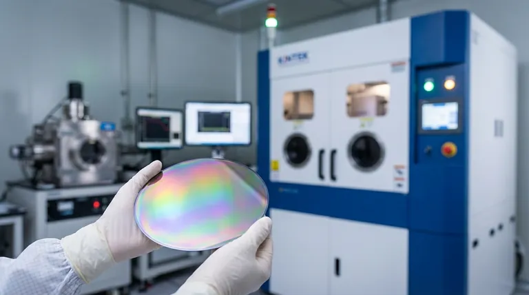
At their core, thin films are microscopic layers of material, ranging from nanometers to several micrometers in thickness, deposited onto a substrate. Their characteristics are not just a smaller version of the bulk material; instead, they possess a unique set of optical, electrical, mechanical, and chemical properties that emerge directly from their extreme thinness and the specific processes used to create them.
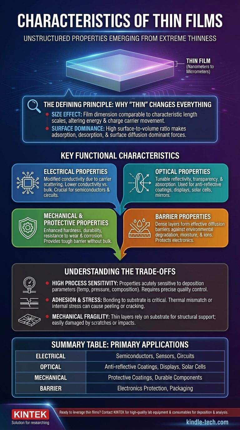
The defining characteristic of a thin film is that its properties are dominated by its surface and dimensional constraints. This "size effect" causes films to behave fundamentally differently than their bulk material counterparts, unlocking novel applications in electronics, optics, and engineering.
The Defining Principle: Why "Thin" Changes Everything
The transition from a three-dimensional bulk material to a quasi-two-dimensional film is the source of its unique behavior. The properties are no longer governed by the bulk material's internal structure alone, but by a new interplay between its surfaces, interfaces, and limited thickness.
The Size Effect
The "size effect" is the most critical concept. It occurs when a physical dimension of the film becomes comparable to or smaller than a characteristic length scale of the material, such as the mean free path of an electron.
This dimensional constraint fundamentally alters how energy and charge carriers move through the material, directly impacting its electrical and thermal conductivity.
Surface Dominance
In a thin film, the ratio of surface area to volume is extraordinarily high. As a result, phenomena that are negligible in bulk materials—such as adsorption, desorption, and surface diffusion—become dominant forces.
The film's interaction with its environment and the substrate it rests on plays a massive role in its overall performance and stability.
Unique Microstructures
Thin films are grown atom by atom or molecule by molecule. This deposition process creates distinct microstructures, including grain boundaries, defects, and internal stresses, that are not typically found in bulk materials.
These structures are not necessarily flaws; they can be precisely engineered to fine-tune the film's properties.
Key Functional Characteristics
Depending on the material and deposition method, thin films can be engineered to serve highly specific functions. They are typically categorized by their primary application, whether electrical, optical, or mechanical.
Electrical Properties
A film's electrical behavior depends on whether it is made from a metal, semiconductor, or insulator. Due to the size effect, charge carriers scatter more frequently off surfaces and grain boundaries.
This leads to a shorter mean free path and generally results in lower electrical conductivity compared to the same material in its bulk form. This effect is crucial in the design of integrated circuits and semiconductor devices.
Optical Properties
Thin films are essential in optics. They can be made anti-reflective for lenses and solar cells or highly reflective for mirrors. The interference of light as it passes through and reflects off the film's surfaces is precisely controlled by its thickness.
Crucially, some films can be both optically transparent and electrically conductive, a property that is the bedrock of modern touch screens, monitors, and solar panels.
Mechanical and Protective Properties
Thin films are often applied to a substrate to enhance its surface. They provide significant benefits like increased durability, hardness, and resistance to corrosion and wear.
These films act as a tough, protective barrier without significantly changing the dimensions of the underlying component. They can also provide purely aesthetic benefits by changing a substrate's color or reflectivity.
Barrier Properties
Because they can be deposited as dense, continuous layers, many thin films are excellent barriers. For example, a silicon nitride film can act as a highly effective diffusion barrier against water molecules and sodium ions.
This property is critical for protecting sensitive electronic components from environmental degradation, ensuring their long-term reliability.
Understanding the Trade-offs
While powerful, thin films present unique engineering challenges. Their performance is inextricably linked to the precision of their manufacturing process.
High Process Sensitivity
A film's final properties are acutely sensitive to the deposition parameters, such as temperature, pressure, and the chemical composition of the plasma or vapor.
Even minor deviations in the manufacturing process can lead to significant variations in performance and yield, making quality control a primary concern.
Adhesion and Stress
A film is only as good as its bond to the substrate. Achieving strong adhesion is a constant challenge, as mismatches in thermal expansion or internal stresses built up during deposition can cause the film to peel or crack.
Mechanical Fragility
While a film can be extremely hard (e.g., diamond-like carbon), it is still a very thin layer. It relies entirely on the underlying substrate for structural support and can be easily damaged by scratches or impacts that penetrate the film.
How to Apply This to Your Goal
The right thin film characteristic is entirely dependent on your objective. The material and deposition method are chosen specifically to achieve a desired outcome.
- If your primary focus is electronics: You will leverage a film's specific conductivity or insulating capacity and its ability to act as a precise barrier in integrated circuits and sensors.
- If your primary focus is optics: You will manipulate a film's thickness and refractive index to create anti-reflective coatings, filters, mirrors, or transparent conductors for displays.
- If your primary focus is mechanical engineering: You will use hard, durable films to enhance a component's surface by providing superior wear resistance, reducing friction, and preventing corrosion.
Ultimately, mastering thin films means controlling matter at the nanoscale to unlock properties that are impossible to achieve in the bulk world.
Summary Table:
| Characteristic | Key Feature | Primary Application |
|---|---|---|
| Electrical | Modified conductivity due to size effect | Semiconductors, sensors, circuits |
| Optical | Tunable reflectivity/transparency | Anti-reflective coatings, displays, solar cells |
| Mechanical | Enhanced hardness and wear resistance | Protective coatings, durable components |
| Barrier | Impermeable to moisture and ions | Electronics protection, packaging |
Ready to leverage the unique properties of thin films in your lab? At KINTEK, we specialize in providing high-quality lab equipment and consumables for precise thin film deposition and analysis. Whether you're developing advanced electronics, optical coatings, or protective surfaces, our solutions ensure reliability and performance. Contact us today to discuss how we can support your laboratory's thin film research and production needs!
Visual Guide
Related Products
- RF PECVD System Radio Frequency Plasma-Enhanced Chemical Vapor Deposition RF PECVD
- Inclined Rotary Plasma Enhanced Chemical Vapor Deposition PECVD Equipment Tube Furnace Machine
- Chemical Vapor Deposition CVD Equipment System Chamber Slide PECVD Tube Furnace with Liquid Gasifier PECVD Machine
- HFCVD Machine System Equipment for Drawing Die Nano-Diamond Coating
- 915MHz MPCVD Diamond Machine Microwave Plasma Chemical Vapor Deposition System Reactor
People Also Ask
- What are the applications of PECVD? Essential for Semiconductors, MEMS, and Solar Cells
- How does RF power create plasma? Achieve Stable, High-Density Plasma for Your Applications
- How are PECVD and CVD different? A Guide to Choosing the Right Thin-Film Deposition Process
- Why is PECVD environment friendly? Understanding the Eco-Friendly Benefits of Plasma-Enhanced Coating
- What is the principle of plasma enhanced chemical vapor deposition? Achieve Low-Temperature Thin Film Deposition