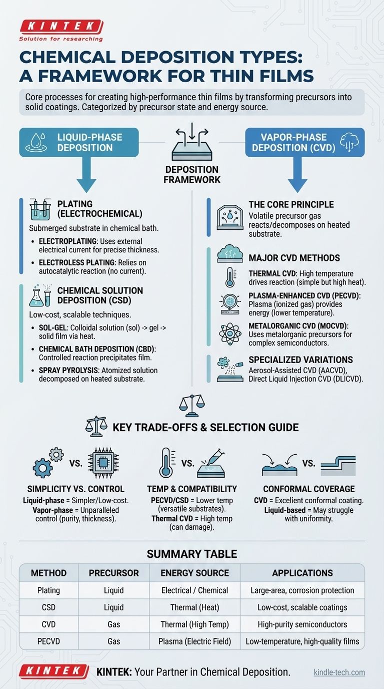
At its core, chemical deposition is a family of processes used to create high-performance thin films and coatings. The primary types are categorized by the physical state of the chemical precursor: liquid-based methods like Plating and Chemical Solution Deposition (CSD), and gas-based methods, most notably Chemical Vapor Deposition (CVD).
The fundamental difference between chemical deposition techniques comes down to two factors: the phase of the precursor material (liquid or gas) and the type of energy (heat, plasma, electricity) used to drive the chemical reaction that forms the final film.
A Framework for Understanding Deposition
All chemical deposition methods share a common goal: to transform a chemical precursor into a solid thin film on the surface of a substrate. The precursor contains the atoms you want to deposit, and a chemical reaction is triggered to leave behind only the desired material.
The major families of these techniques are distinguished by whether that precursor starts as a liquid or a gas. This single difference has profound implications for the equipment, cost, and quality of the resulting film.
Liquid-Phase Deposition: Plating and Solutions
These methods are often characterized by simpler equipment and lower operating temperatures, making them versatile for a wide range of applications. They all begin with the substrate being exposed to a chemical precursor dissolved in a liquid solution.
Plating (Electrochemical Deposition)
Plating is one of the oldest and most common deposition techniques. It involves submerging a substrate in a chemical bath where ions of the coating material are present.
Electroplating uses an external electrical current to drive the deposition of these ions onto the substrate's surface, offering precise control over the film's thickness.
Electroless Plating achieves the same result without an external current. Instead, it relies on an autocatalytic chemical reaction within the solution itself to deposit the material.
Chemical Solution Deposition (CSD)
CSD is a broad category that encompasses several low-cost, scalable techniques.
The Sol-Gel Technique involves creating a stable colloidal solution (a "sol") that is applied to a substrate. Through a heat treatment, the sol is transformed into a gel and then a dense, solid film.
Chemical Bath Deposition (CBD) works by simply immersing a substrate into a solution where a controlled chemical reaction slowly precipitates a solid film onto its surface.
Spray Pyrolysis is a technique where a precursor solution is atomized into a fine spray and directed onto a heated substrate. The droplets undergo a thermal decomposition upon contact, forming the desired film.
Vapor-Phase Deposition: The World of CVD
Chemical Vapor Deposition (CVD) is the cornerstone of modern microelectronics and advanced materials manufacturing. It is renowned for its ability to produce extremely pure, uniform, and conformal coatings.
The Core Principle of CVD
In any CVD process, a volatile precursor gas is introduced into a reaction chamber containing the substrate. Energy is applied, causing the gas to react or decompose on the hot substrate surface, leaving behind a high-quality solid film.
Thermal CVD
This is the most fundamental form of CVD, where high temperature (thermal energy) is the sole driver for the chemical reaction. Its simplicity is effective, but the high temperatures required can damage sensitive substrates.
Plasma-Enhanced CVD (PECVD)
To overcome the temperature limitations of thermal CVD, PECVD uses an electric field to generate a plasma (an ionized gas). This highly reactive plasma provides the energy for the deposition reaction, allowing for high-quality films to be grown at much lower temperatures.
Metalorganic CVD (MOCVD)
MOCVD is a highly precise subtype of CVD that uses metalorganic compounds as precursors. It is a critical process for manufacturing complex semiconductor devices like LEDs and high-power transistors.
Other Specialized CVD Methods
The versatility of the CVD concept has led to many specialized variations, including Aerosol-Assisted CVD (AACVD), which uses an aerosol to deliver the precursor, and Direct Liquid Injection CVD (DLICVD), where a liquid precursor is vaporized just before entering the chamber.
Understanding the Key Trade-offs
No single deposition method is universally superior. The choice always involves a balance between cost, quality, and material compatibility.
Simplicity vs. Control
Liquid-phase methods like CSD and plating generally involve simpler, lower-cost equipment and are easier to scale to large areas. However, vapor-phase methods like CVD offer unparalleled control over film purity, thickness, and structure, which is essential for high-performance electronics.
Temperature and Substrate Compatibility
High temperatures used in thermal CVD can damage materials like plastics or pre-existing electronic components. This is where methods like PECVD, plating, and many CSD techniques are advantageous, as their lower processing temperatures are compatible with a wider range of substrates.
Conformal Coverage
CVD processes excel at creating conformal coatings, meaning the film deposits with a perfectly uniform thickness over complex, three-dimensional surfaces. Liquid-based methods can struggle with this, as surface tension and fluid dynamics may lead to uneven coverage in trenches or on sharp corners.
Choosing the Right Deposition Method
Your choice depends entirely on the requirements of your final product. Use these guidelines to steer your decision.
- If your primary focus is low-cost, large-area coating: Consider CSD methods like spray pyrolysis or plating, which are highly scalable and cost-effective.
- If your primary focus is maximum purity and uniformity for semiconductors: A specialized CVD process like MOCVD or PECVD is almost always the correct choice.
- If your primary focus is coating a heat-sensitive substrate like a polymer: Look to low-temperature methods such as PECVD, electroless plating, or certain sol-gel processes.
By understanding the relationship between the precursor's state and the required energy, you can effectively navigate these techniques to find the optimal solution for your engineering challenge.
Summary Table:
| Deposition Method | Precursor State | Key Energy Source | Primary Applications |
|---|---|---|---|
| Plating (Electro/Electroless) | Liquid | Electrical / Chemical | Large-area coatings, corrosion protection |
| Chemical Solution Deposition (CSD) | Liquid | Thermal (Heat) | Low-cost, scalable coatings |
| Chemical Vapor Deposition (CVD) | Gas | Thermal (High Temp) | High-purity semiconductors, microelectronics |
| Plasma-Enhanced CVD (PECVD) | Gas | Plasma (Electric Field) | Low-temperature, high-quality films |
Need expert guidance on selecting the right deposition method for your lab? KINTEK specializes in providing high-quality lab equipment and consumables for all your chemical deposition needs—from robust plating systems to advanced CVD reactors. Our team can help you optimize your process for purity, cost, and substrate compatibility. Contact us today to discuss your specific application and discover how our solutions can enhance your research and production outcomes!
Visual Guide
Related Products
- Chemical Vapor Deposition CVD Equipment System Chamber Slide PECVD Tube Furnace with Liquid Gasifier PECVD Machine
- Microwave Plasma Chemical Vapor Deposition MPCVD Machine System Reactor for Lab and Diamond Growth
- RF PECVD System Radio Frequency Plasma-Enhanced Chemical Vapor Deposition RF PECVD
- Customer Made Versatile CVD Tube Furnace Chemical Vapor Deposition Chamber System Equipment
- HFCVD Machine System Equipment for Drawing Die Nano-Diamond Coating
People Also Ask
- How expensive is chemical vapor deposition? Understanding the True Cost of High-Performance Coating
- Why is Chemical Vapor Deposition (CVD) equipment uniquely suited for constructing hierarchical superhydrophobic structures?
- What happens during deposition chemistry? Building Thin Films from Gaseous Precursors
- What are the core advantages of PE-CVD in OLED encapsulation? Protect Sensitive Layers with Low-Temp Film Deposition
- How are carbon nanotubes grown? Master Scalable Production with Chemical Vapor Deposition


