High Density Plasma Chemical Vapour Deposition (HDPCVD) is a sophisticated evolution of standard deposition techniques designed to solve critical scaling challenges in semiconductor manufacturing. It offers substantial improvements in film densification, accelerated growth rates, and the ability to fill deep, narrow trenches without defects. These capabilities make it the primary technology used for shallow trench isolation (STI) in the fabrication of CMOS integrated circuits.
Core Takeaway HDPCVD succeeds where traditional methods fail by employing simultaneous deposition and etching within the same chamber. This unique mechanism prevents the formation of voids and "pinch-offs" in high-aspect-ratio gaps smaller than 0.8 microns, ensuring the structural integrity required for modern microelectronics.
The Engineering Behind the Improvements
Standard Plasma Enhanced Chemical Vapour Deposition (PECVD) often struggles as circuit features shrink. HDPCVD addresses these limitations through higher plasma density and a dual-action process.
Superior Gap Filling
The most critical improvement of HDPCVD is its "gap-filling" capability. In traditional processes, material builds up at the top of a trench too quickly, closing it off and leaving a void inside (a "pinch-off").
HDPCVD eliminates this by filling trenches and holes that have high aspect ratios. It is specifically effective for gaps smaller than 0.8 microns, ensuring a solid, void-free fill.
Simultaneous Deposition and Etching
The mechanism behind this superior filling is the concurrent execution of deposition and etching.
As the film deposits, the system simultaneously etches the material. This keeps the top of the trench open longer, allowing the depositing material to reach the bottom of the trench completely before the top closes.
Enhanced Film Densification
HDPCVD produces films with significantly higher density compared to standard PECVD.
This results in higher-quality films that are more robust and reliable. Notably, this improved quality is achieved even at lower deposition temperatures, preserving the thermal budget of the device manufacturing process.
Independent Process Control
Operators gain precise control over the deposition environment.
HDPCVD systems allow for nearly independent control of ion flux and ion energy. This granularity is essential for tuning the process to specific trench geometries and material requirements.
Primary Applications in Electronics
While HDPCVD is a versatile tool, its application is concentrated on specific, high-value steps in semiconductor fabrication.
Shallow Trench Isolation (STI)
The definitive application for HDPCVD is Shallow Trench Isolation.
In CMOS integrated circuits, electrical components must be isolated from one another to prevent interference. HDPCVD is used to fill the trenches created between these components with dielectric material, providing effective electrical isolation.
Advanced CMOS Fabrication
Because modern CMOS devices require densely packed components, the trenches used for isolation are extremely narrow.
HDPCVD is indispensable here because it is one of the few methods capable of filling these microscopic isolation structures without creating defects that would cause circuit failure.
Operational Flexibility and Trade-offs
When selecting equipment for a fabrication line, resource constraints are often just as important as technical capability. HDPCVD offers unique advantages in system architecture.
Dual-Function Capability
A significant operational advantage is the system's convertibility.
An HDPCVD configuration can often be converted into an Inductively Coupled Plasma-Reactive Ion Etching (ICP-RIE) system. This allows the same hardware footprint to perform plasma etching when not being used for deposition.
Managing Budget and Footprint
For facilities with limited floor space or capital budgets, this versatility is a major trade-off benefit.
Instead of purchasing two distinct dedicated tools, a facility can utilize the convertible nature of the HDPCVD system to handle multiple process steps, maximizing the return on investment for the equipment.
Making the Right Choice for Your Goal
To maximize the value of HDPCVD, align its specific capabilities with your fabrication requirements.
- If your primary focus is Device Scaling and Quality: Prioritize HDPCVD for its ability to fill high-aspect-ratio gaps (<0.8 microns) and create high-density films for Shallow Trench Isolation (STI).
- If your primary focus is Facility Efficiency: Leverage the system's ability to convert to an ICP-RIE etcher to save floor space and reduce capital expenditure.
HDPCVD is not just a deposition method; it is a structural solution for preventing defects in the increasingly microscopic architecture of modern integrated circuits.
Summary Table:
| Feature | Improvement/Benefit | Primary Application |
|---|---|---|
| Gap Filling | Fills trenches < 0.8 microns without voids | Shallow Trench Isolation (STI) |
| Deposition Style | Simultaneous deposition and etching | High-aspect-ratio structures |
| Film Quality | Higher density at lower temperatures | Advanced CMOS fabrication |
| Process Control | Independent ion flux and energy control | Precision semiconductor tuning |
| Hardware | Convertible to ICP-RIE etching system | Facility space & budget optimization |
Elevate Your Semiconductor Fabrication with KINTEK Precision
Facing challenges with void-free gap filling or film densification in your microelectronics research? KINTEK specializes in high-performance laboratory equipment, providing the advanced solutions needed for next-generation material science.
From our cutting-edge CVD and PECVD systems to our comprehensive range of high-temperature furnaces and vacuum solutions, we empower researchers and manufacturers to achieve superior structural integrity in every layer. Our portfolio also features high-pressure reactors, battery research tools, and essential consumables like ceramics and crucibles tailored for rigorous lab environments.
Ready to optimize your deposition process? Contact KINTEK today to discuss how our specialized equipment can enhance your lab's efficiency and device performance.
Related Products
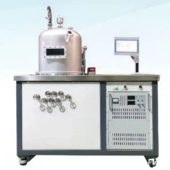
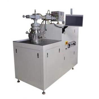
- HFCVD Machine System Equipment for Drawing Die Nano-Diamond Coating
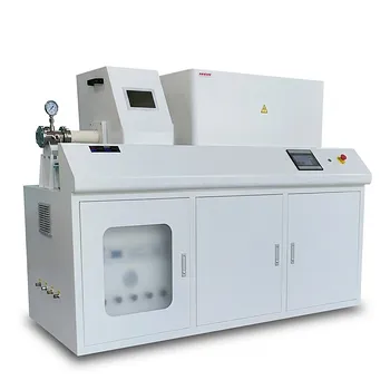
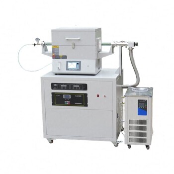
- Inclined Rotary Plasma Enhanced Chemical Vapor Deposition PECVD Equipment Tube Furnace Machine
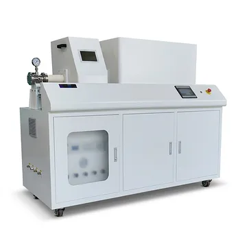
- Chemical Vapor Deposition CVD Equipment System Chamber Slide PECVD Tube Furnace with Liquid Gasifier PECVD Machine
- Inclined Rotary Plasma Enhanced Chemical Vapor Deposition PECVD Equipment Tube Furnace Machine
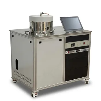
- Microwave Plasma Chemical Vapor Deposition MPCVD Machine System Reactor for Lab and Diamond Growth
People Also Ask
- What types of substrates are used in CVD to facilitate graphene films? Optimize Graphene Growth with the Right Catalyst
- How expensive is chemical vapor deposition? Understanding the True Cost of High-Performance Coating
- What is the hot filament chemical vapour deposition of diamond? A Guide to Synthetic Diamond Coating
- What is the chemical vapor deposition growth process? Build Superior Thin Films from the Atom Up
- What is the function of tungsten filaments in HFCVD? Powering Diamond Film Synthesis with Thermal Excitation
