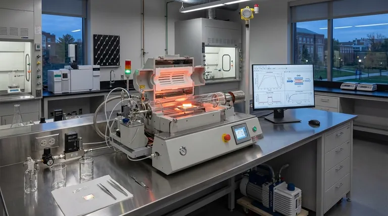
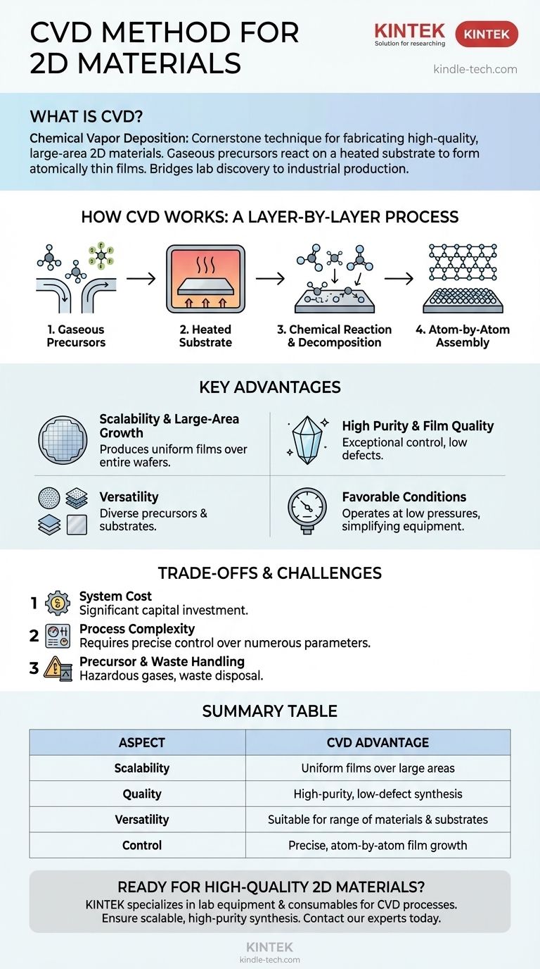
Chemical Vapor Deposition (CVD) is a cornerstone technique for fabricating high-quality, large-area 2D materials. It is a process where gaseous precursor materials are introduced into a reaction chamber, where they react and decompose on a heated substrate to form an atomically thin, solid film. This method allows for precise, atom-by-atom control over the growth of materials, making it a powerful and widely used approach for producing thin films.
CVD bridges the gap between lab-scale discovery and industrial-scale production of 2D materials. Its fundamental advantage lies in its unique ability to grow high-quality, uniform films over large areas, a critical requirement for practical applications.
How CVD Fundamentally Works
The elegance of the CVD process is in its simplicity. It involves transforming gas-phase chemicals into a solid, layer-by-layer, onto a surface.
The Gaseous Precursors
The process begins with one or more precursor gases. These gases contain the atoms required for the final 2D material (e.g., methane for graphene's carbon, or tungsten hexafluoride and hydrogen sulfide for tungsten disulfide).
The Heated Substrate
These gases are introduced into a reaction chamber containing a substrate, which is heated to a high temperature. This substrate acts as the surface where the 2D material will form.
The Chemical Reaction
The high temperature of the substrate provides the energy needed to trigger a chemical reaction. The precursor gases decompose, and the desired atoms are deposited onto the substrate's surface, assembling into the atomically thin crystal structure of the 2D material.
Atom-by-Atom Assembly
This deposition happens in a highly controlled manner, effectively "growing" the 2D material one atomic layer at a time. The unreacted gases and chemical byproducts are then exhausted from the chamber.
The Key Advantages of the CVD Method
CVD has become a dominant method for 2D material synthesis because of several distinct advantages that are difficult to achieve with other techniques.
Scalability and Large-Area Growth
This is arguably the most significant advantage. CVD can produce uniform, high-quality 2D material films over large areas (e.g., entire wafers), which is essential for manufacturing electronic devices.
High Purity and Film Quality
Because the process uses highly refined precursor gases in a controlled environment, it offers exceptional control over chemical impurities. This results in films with very high clarity and fewer defects.
Versatility in Materials and Substrates
The high-temperature nature of the reaction allows for a diverse range of precursor materials to be used. This flexibility makes CVD suitable for synthesizing a wide variety of 2D materials on different substrates.
Favorable Operating Conditions
Unlike some synthesis methods that require extremely high pressures, CVD typically operates at pressures well below standard atmospheric pressure. This simplifies the engineering requirements for the equipment.
Understanding the Trade-offs and Challenges
While powerful, the CVD method is not without its complexities and potential drawbacks. An objective assessment requires understanding these limitations.
System Cost
Automated, commercial-grade CVD systems are sophisticated instruments and can represent a significant capital investment. This cost can be a barrier for some academic research groups or startups.
Process Complexity
Achieving a perfectly uniform, single-layer film requires precise control over numerous parameters. Temperature, pressure, gas flow rates, and timing must be meticulously managed to get repeatable, high-quality results.
Precursor and Waste Handling
CVD often relies on precursor gases that can be hazardous or expensive. The process also produces waste materials and byproducts that must be handled and disposed of safely.
Making the Right Choice for Your Goal
Selecting a synthesis method depends entirely on your end goal. CVD is the optimal choice for specific, demanding applications.
- If your primary focus is large-scale, uniform production: CVD is the leading method due to its proven ability to grow consistent films over large substrates, making it ideal for industrial applications.
- If your primary focus is achieving the highest material purity: CVD offers exceptional control over the chemical environment, allowing you to create materials with minimal impurities and defects.
- If your primary focus is research and development on a budget: Consider exploring open-source designs for CVD systems, as purchasing commercial units can be cost-prohibitive.
Ultimately, mastering the CVD process is essential for advancing 2D materials from the laboratory to real-world applications.
Summary Table:
| Aspect | CVD Advantage |
|---|---|
| Scalability | Produces uniform films over large areas (e.g., entire wafers) |
| Quality | Enables high-purity, low-defect material synthesis |
| Versatility | Suitable for a wide range of 2D materials and substrates |
| Control | Offers precise, atom-by-atom control over film growth |
Ready to integrate high-quality 2D materials into your research or production? KINTEK specializes in providing the lab equipment and consumables you need to successfully implement CVD processes. Our expertise ensures you have the right tools for scalable, high-purity synthesis. Contact our experts today to discuss your specific laboratory requirements and how we can support your project's success.
Visual Guide
Related Products
- Chemical Vapor Deposition CVD Equipment System Chamber Slide PECVD Tube Furnace with Liquid Gasifier PECVD Machine
- Customer Made Versatile CVD Tube Furnace Chemical Vapor Deposition Chamber System Equipment
- HFCVD Machine System Equipment for Drawing Die Nano-Diamond Coating
- Split Chamber CVD Tube Furnace with Vacuum Station Chemical Vapor Deposition System Equipment Machine
- Multi Heating Zones CVD Tube Furnace Machine Chemical Vapor Deposition Chamber System Equipment
People Also Ask
- Why is Chemical Vapor Deposition (CVD) equipment uniquely suited for constructing hierarchical superhydrophobic structures?
- What happens during deposition chemistry? Building Thin Films from Gaseous Precursors
- What are the processes of vapor phase deposition? Understand CVD vs. PVD for Superior Thin Films
- What types of substrates are used in CVD to facilitate graphene films? Optimize Graphene Growth with the Right Catalyst
- What is plasma enhanced chemical vapor deposition PECVD equipment? A Guide to Low-Temperature Thin Film Deposition


