In short, deposition technology is a foundational manufacturing process used to apply an ultra-thin layer of material—a "thin film"—onto a surface. It is the essential technique behind the creation of modern electronics like semiconductors, functional coatings that protect parts from wear, and high-performance optical devices like solar panels and lenses.
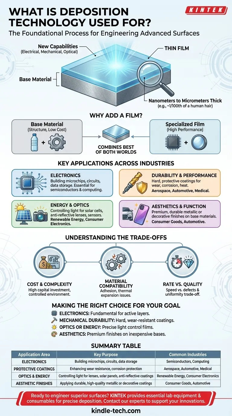
The core purpose of deposition is not simply to coat an object, but to fundamentally alter the properties of its surface. It grants a material new capabilities—be it electrical, mechanical, or optical—that the underlying object does not possess on its own.
The Core Principle: Engineering a Surface
Deposition technology is about precision engineering at a microscopic, and often atomic, scale. It allows us to build complex structures layer by layer.
What Is a "Thin Film"?
A thin film is a layer of material ranging from a few nanometers (a handful of atoms) to several micrometers thick. For perspective, a single human hair is about 70 micrometers thick.
These films are so thin that they are often transparent and do not change the physical dimensions of an object in a noticeable way. Their value comes from their carefully controlled properties.
Why Add a Film?
It is often impractical, impossible, or too expensive to make an entire object out of a material with specific desired properties.
Deposition allows us to combine the best of both worlds: the structural integrity and low cost of a base material (like glass, plastic, or steel) with the high-performance surface properties of a different, specialized material.
Key Applications Across Industries
The ability to engineer a surface has unlocked capabilities across nearly every modern industry. The applications can be broadly understood in a few key categories.
Powering Modern Electronics
This is arguably the most significant application. The microchips that power our computers and smartphones are built by depositing and then etching dozens of successive thin films of conducting, insulating, and semiconducting materials to create microscopic circuits.
Likewise, the data on hard drives and other storage media is held in precisely deposited magnetic thin films.
Enhancing Durability and Performance
Deposition is used to apply hard, protective coatings to tools and components. A "super hard" film of a material like titanium nitride can be deposited on a steel drill bit, making it last much longer without changing the steel itself.
These films also provide crucial resistance to corrosion, heat, and oxidation for components used in aerospace, automotive, and medical industries.
Capturing and Controlling Energy
Solar panels (photovoltaics) work by using a stack of thin films engineered to absorb sunlight and convert it into electricity.
Optical coatings are another major use. The anti-reflective coating on your eyeglasses is a thin film designed to reduce glare. Similar films are essential for high-performance lenses, mirrors, and sensors.
Improving Aesthetics and Function
Many metallic finishes on plastics and other materials are not paint, but thin films applied through deposition. This provides a durable, high-quality decorative finish. Often, these coatings also add functional benefits like scratch resistance.
Understanding the Trade-offs
While powerful, deposition is not a simple solution. It involves significant technical challenges and economic considerations.
Cost and Complexity
Deposition equipment, which often requires high-vacuum chambers and sophisticated power sources, is a major capital investment. The process demands a highly controlled, clean environment, adding to operational complexity and cost.
Material Compatibility
Successfully depositing a film requires strong adhesion to the underlying material, known as the substrate. Mismatches in thermal expansion or chemical incompatibility between the film and substrate can cause the film to peel, crack, or fail over time.
Rate vs. Quality
In manufacturing, there is often a direct trade-off between the speed of deposition and the quality of the final film. Depositing faster can increase throughput but may result in a film with more defects and less uniform properties, impacting the performance of the final product.
Making the Right Choice for Your Goal
When considering deposition, your primary objective will determine your approach and the specific technology you might use.
- If your primary focus is creating electronic devices: Deposition is the non-negotiable, fundamental process for building the active layers of semiconductors, circuits, and data storage media.
- If your primary focus is improving mechanical durability: Use deposition to apply hard, wear-resistant, or anti-corrosion coatings without changing the bulk material of your component.
- If your primary focus is optics or energy: Leverage deposition to create films that precisely control the reflection, transmission, or absorption of light for applications like lenses and solar cells.
- If your primary focus is aesthetics: Deposition can provide premium, durable metallic or ceramic finishes on inexpensive base materials like plastic.
Ultimately, deposition technology gives us the power to engineer material properties at the nanoscale, unlocking a world of advanced capabilities.
Summary Table:
| Application Area | Key Purpose | Common Industries |
|---|---|---|
| Electronics | Building microchips, circuits, and data storage | Semiconductors, Computing |
| Protective Coatings | Enhancing wear resistance, corrosion protection | Aerospace, Automotive, Medical |
| Optics & Energy | Controlling light for lenses, solar panels, anti-reflective coatings | Renewable Energy, Consumer Electronics |
| Aesthetic Finishes | Applying durable, high-quality metallic or decorative coatings | Consumer Goods, Automotive |
Ready to engineer superior surfaces for your products?
KINTEK specializes in providing the lab equipment and consumables essential for precise deposition processes. Whether you are developing new semiconductors, durable protective coatings, or advanced optical devices, our expertise can help you achieve the high-quality, reliable thin films your projects demand.
Contact our experts today to discuss how we can support your laboratory's deposition technology needs and help you bring your innovations to life.
Visual Guide
Related Products
- Chemical Vapor Deposition CVD Equipment System Chamber Slide PECVD Tube Furnace with Liquid Gasifier PECVD Machine
- RF PECVD System Radio Frequency Plasma-Enhanced Chemical Vapor Deposition RF PECVD
- Inclined Rotary Plasma Enhanced Chemical Vapor Deposition PECVD Equipment Tube Furnace Machine
- Inclined Rotary Plasma Enhanced Chemical Vapor Deposition PECVD Equipment Tube Furnace Machine
- Electron Beam Evaporation Coating Oxygen-Free Copper Crucible and Evaporation Boat
People Also Ask
- What is plasma enhanced chemical vapor deposition PECVD equipment? A Guide to Low-Temperature Thin Film Deposition
- What are the core advantages of PE-CVD in OLED encapsulation? Protect Sensitive Layers with Low-Temp Film Deposition
- How expensive is chemical vapor deposition? Understanding the True Cost of High-Performance Coating
- Why is Chemical Vapor Deposition (CVD) equipment uniquely suited for constructing hierarchical superhydrophobic structures?
- What types of substrates are used in CVD to facilitate graphene films? Optimize Graphene Growth with the Right Catalyst


