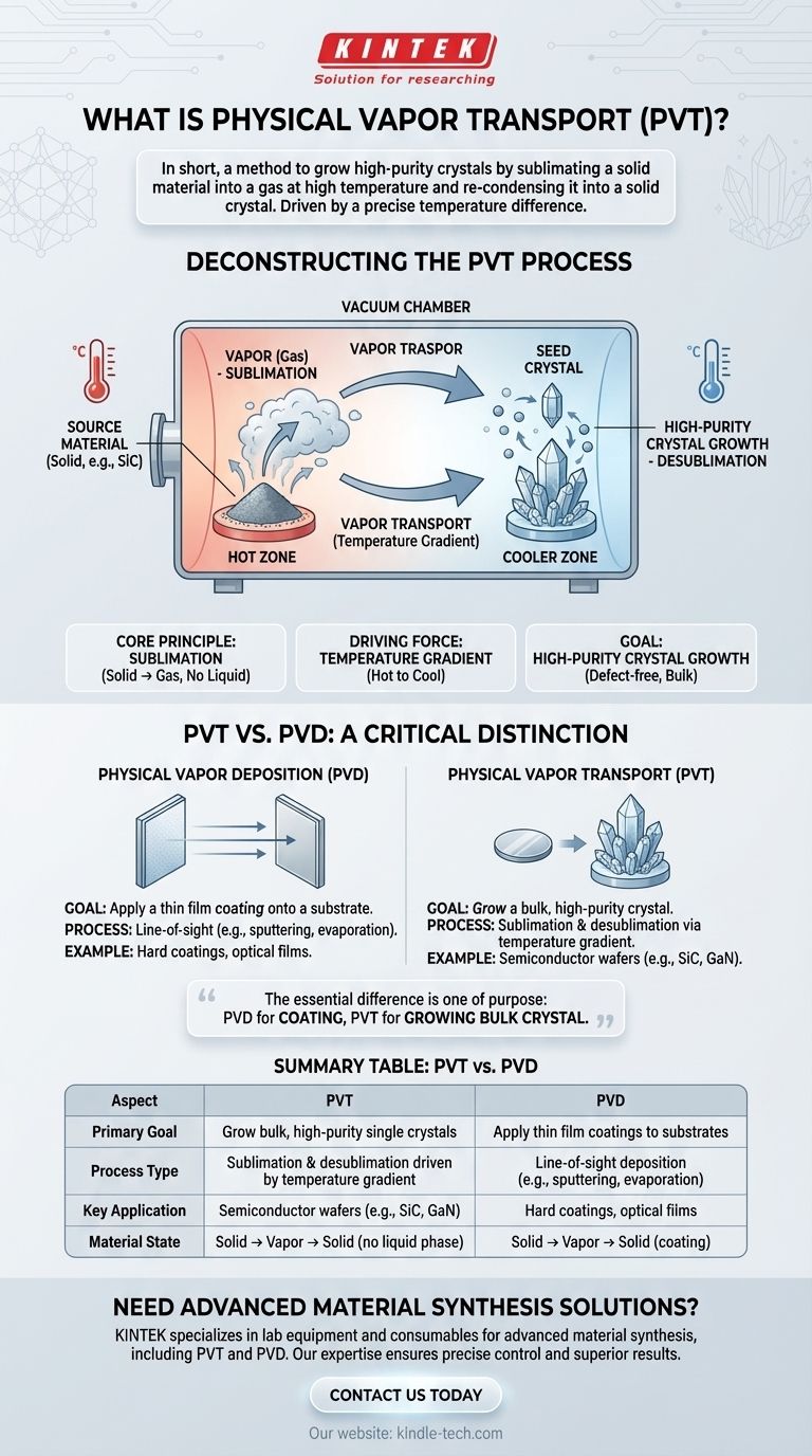
In short, Physical Vapor Transport (PVT) is a method used to grow high-purity crystals by sublimating a solid material into a gas at a high temperature and then allowing it to re-condense into a solid crystal in a cooler region. It is a purification and growth technique driven by a precise temperature difference. This is distinct from Physical Vapor Deposition (PVD), which is a broader term for coating a surface with a thin film.
The essential difference is one of purpose. Physical Vapor Deposition (PVD) is primarily used to apply a thin coating onto a substrate. Physical Vapor Transport (PVT) is a specialized process used to grow a bulk, high-purity crystal from a source material.

Deconstructing the Vapor Transport Process
To truly understand PVT, you must visualize it as a closed-system journey where material changes from solid to gas and back to a more perfect solid. It's less about coating a foreign object and more about refining and recrystallizing a material.
The Core Principle: Sublimation
At the heart of PVT is sublimation, the direct transition of a substance from a solid to a gas phase without passing through a liquid phase.
The process begins with a source material (e.g., silicon carbide powder) which is heated in a controlled environment, like a vacuum chamber, to a temperature high enough for it to turn into a vapor.
The Driving Force: The Temperature Gradient
This vapor doesn't stay static. The chamber is designed to have a specific temperature gradient—a hot zone where the source material is and a slightly cooler zone where a "seed crystal" is located.
Gas molecules naturally move from the hotter, higher-pressure area to the cooler, lower-pressure area. This movement is the "transport" in Physical Vapor Transport.
The Goal: High-Purity Crystal Growth
When the gaseous material reaches the cooler seed crystal, it re-condenses directly back into a solid. This process, called desublimation, is highly controlled.
The atoms arrange themselves onto the seed crystal's existing lattice, extending its structure. This allows for the growth of very large, single crystals with extremely low defect density, which is critical for high-performance electronics.
PVT vs. PVD: A Critical Distinction
The terms are often confused, but their objectives are fundamentally different. The reference materials you provided primarily describe PVD, which is a broader category of techniques.
Physical Vapor Deposition (PVD): Coating a Surface
PVD is a line-of-sight process designed to apply a thin film onto a substrate. As the references note, this includes methods like evaporation and sputtering.
The goal is to enhance the surface properties of an object, such as applying a hard, corrosion-resistant coating to a tool bit or an optical film onto a lens. The deposited film is often a different material than the substrate it coats.
Physical Vapor Transport (PVT): Growing a Bulk Material
PVT is a specific crystal growth method. The goal is not to coat a dissimilar object, but to grow a large, defect-free bulk crystal of the source material itself.
Think of it as taking raw, powdered material and re-forming it into a perfect, monolithic crystal structure. For example, PVT is the dominant method for producing the large silicon carbide (SiC) boules that are later sliced into wafers for power electronics.
Understanding the Trade-offs and Context
Choosing between PVT, PVD, or other methods like Chemical Vapor Deposition (CVD) depends entirely on the material and the desired outcome.
Why Not Just Melt It?
Many advanced materials, like Silicon Carbide (SiC) or Gallium Nitride (GaN), cannot be easily grown from a molten state. They may decompose or have melting points so high that they are impractical to handle as liquids.
PVT bypasses the liquid phase entirely, making it possible to create high-quality crystals of materials that are otherwise difficult to form.
The Role of Chemical Processes (CVD)
If the goal is to form a compound material from different precursor gases, you need Chemical Vapor Deposition (CVD). In CVD, gases are introduced into a chamber where they chemically react to form a solid film on a substrate.
As noted in the references, Plasma-Enhanced CVD (PECVD) uses a plasma to facilitate these reactions at lower temperatures. This is fundamentally different from PVT and PVD, which are physical processes that do not involve chemical reactions to create the material.
Equipment Commonalities and Key Differences
All these processes occur in a vacuum chamber with pumps and gas flow controllers. However, a PVT system's design is dominated by the need to create and maintain a precise, stable temperature gradient between the source and the seed. PVD systems focus on the source-to-substrate geometry, and CVD systems require complex gas mixing and delivery systems for the chemical precursors.
Making the Right Choice for Your Goal
Understanding the end goal is the key to distinguishing between these powerful material science techniques.
- If your primary focus is to apply a thin, durable coating onto a part: You are describing a Physical Vapor Deposition (PVD) process.
- If your primary focus is to grow a large, high-purity single crystal from a solid source: The method you need is Physical Vapor Transport (PVT).
- If your primary focus is to synthesize a film by reacting precursor gases on a surface: You require a form of Chemical Vapor Deposition (CVD).
Ultimately, choosing the right technique begins with clearly defining whether you intend to coat, grow, or react your material.
Summary Table:
| Aspect | Physical Vapor Transport (PVT) | Physical Vapor Deposition (PVD) |
|---|---|---|
| Primary Goal | Grow bulk, high-purity single crystals | Apply thin film coatings to substrates |
| Process Type | Sublimation & desublimation driven by temperature gradient | Line-of-sight deposition (e.g., sputtering, evaporation) |
| Key Application | Semiconductor wafers (e.g., SiC, GaN) | Hard coatings, optical films |
| Material State | Solid → Vapor → Solid (no liquid phase) | Solid → Vapor → Solid (coating) |
Need to Grow High-Purity Crystals or Apply Advanced Coatings?
KINTEK specializes in lab equipment and consumables for advanced material synthesis. Whether you're developing next-generation semiconductors with PVT or enhancing surface properties with PVD, our expertise and reliable equipment ensure precise control and superior results.
Contact us today to discuss your specific needs and discover how KINTEK can support your laboratory's success.
Visual Guide
Related Products
- Chemical Vapor Deposition CVD Equipment System Chamber Slide PECVD Tube Furnace with Liquid Gasifier PECVD Machine
- RF PECVD System Radio Frequency Plasma-Enhanced Chemical Vapor Deposition RF PECVD
- Customer Made Versatile CVD Tube Furnace Chemical Vapor Deposition Chamber System Equipment
- Customizable PTFE Wafer Carriers for Semiconductor and Lab Applications
- Inclined Rotary Plasma Enhanced Chemical Vapor Deposition PECVD Equipment Tube Furnace Machine
People Also Ask
- What is the chemical vapor deposition growth process? Build Superior Thin Films from the Atom Up
- How are carbon nanotubes grown? Master Scalable Production with Chemical Vapor Deposition
- What is plasma enhanced chemical vapor deposition PECVD equipment? A Guide to Low-Temperature Thin Film Deposition
- Why is Chemical Vapor Deposition (CVD) equipment uniquely suited for constructing hierarchical superhydrophobic structures?
- What happens during deposition chemistry? Building Thin Films from Gaseous Precursors