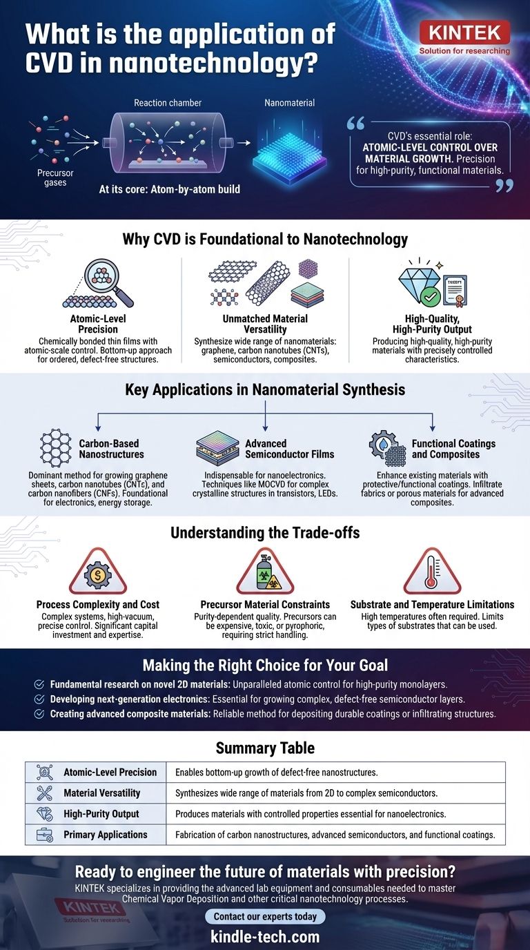
At its core, Chemical Vapor Deposition (CVD) is a cornerstone of modern nanotechnology. It is a highly versatile process used to build nanostructures and ultra-thin films atom-by-atom. This technique is critical for fabricating high-performance materials like graphene and carbon nanotubes, which are essential for applications in nanoelectronics, medicine, and advanced composites.
CVD's essential role in nanotechnology stems from its unique ability to provide atomic-level control over material growth. This precision allows scientists to engineer high-purity, functional materials with specific properties that are impossible to achieve with bulk manufacturing methods.
Why CVD is Foundational to Nanotechnology
CVD is not just one technique but a versatile platform for building materials from the ground up. Its widespread adoption is due to a combination of precision, versatility, and the quality of the final product.
Atomic-Level Precision
CVD allows for the deposition of chemically bonded thin films with atomic-scale control.
This process involves introducing precursor gases into a reaction chamber, which then decompose and react on a substrate surface to form the desired material one layer of atoms at a time.
This bottom-up approach is the key to creating the ordered, defect-free structures required for nano-scale devices.
Unmatched Material Versatility
The CVD process can be adapted to create an incredibly wide range of nanomaterials.
It is used to synthesize simple monoatomic layers like graphene, complex carbon structures like carbon nanotubes (CNTs), and intricate crystalline layers for semiconductors.
Furthermore, it can produce composite films, intermetallic oxides, and other hybrid structures, making it invaluable across scientific disciplines.
High-Quality, High-Purity Output
For nanotechnology applications, material purity is paramount. Even tiny impurities or structural defects can drastically alter a material's properties.
CVD is renowned for producing high-quality, high-purity materials with precisely controlled characteristics.
By carefully managing process parameters like temperature, pressure, and gas flow rates in a high-pressure reactor, researchers can create materials with enhanced strength, specific catalytic activity, or tailored electrical conductivity.
Key Applications in Nanomaterial Synthesis
CVD's capabilities translate directly into the fabrication of the most important materials in the nanotechnology toolkit. Its applications are central to advancing next-generation technology.
Carbon-Based Nanostructures
CVD is the dominant method for synthesizing carbon-based nanomaterials.
It is extensively used to grow graphene sheets, carbon nanotubes (CNTs), and carbon nanofibers (CNFs), which are foundational materials for research in electronics, energy storage, and material science.
Advanced Semiconductor Films
In the field of nanoelectronics, CVD is indispensable.
Specialized techniques like Metalorganic Chemical Vapor Deposition (MOCVD) are used to grow complex, multi-layered crystalline structures on semiconductor wafers. These layers form the basis of modern transistors, LEDs, and power electronics.
Functional Coatings and Composites
Beyond building standalone structures, CVD is used to enhance existing materials.
The process can create protective or functional coatings on a variety of surfaces. It is also used to infiltrate fabrics or porous materials with new elements, creating advanced composites with unique properties.
Understanding the Trade-offs
While powerful, CVD is a sophisticated technique with inherent complexities that must be managed. Understanding its limitations is key to successful application.
Process Complexity and Cost
CVD systems, particularly those for high-purity semiconductor growth, are complex and expensive.
They often require high-vacuum environments, precise temperature controls, and sophisticated gas handling systems, which demand significant capital investment and operational expertise.
Precursor Material Constraints
The quality of the final nanomaterial is directly dependent on the purity of the precursor gases used.
These precursors can be expensive, highly toxic, or pyrophoric (igniting on contact with air), which introduces considerable safety, handling, and logistical challenges.
Substrate and Temperature Limitations
Many CVD processes require very high temperatures to facilitate the necessary chemical reactions.
This can limit the types of substrate materials that can be used, as some may melt, deform, or react undesirably under the deposition conditions.
Making the Right Choice for Your Goal
The decision to use CVD depends entirely on the required material properties and the end goal of your project.
- If your primary focus is fundamental research on novel 2D materials: CVD provides the unparalleled atomic-level control necessary to synthesize high-purity monolayers like graphene or transition metal dichalcogenides.
- If your primary focus is developing next-generation electronics: Specialized CVD techniques are essential for growing the complex, defect-free crystalline layers required for high-performance semiconductor devices.
- If your primary focus is creating advanced composite materials: CVD offers a reliable method for depositing durable, functional coatings or infiltrating existing structures to engineer materials with enhanced properties.
Ultimately, mastering CVD is about harnessing its precision to engineer materials from the atom up, enabling solutions to tomorrow's technological challenges.
Summary Table:
| Key Aspect | Why It Matters for Nanotechnology |
|---|---|
| Atomic-Level Precision | Enables bottom-up growth of defect-free nanostructures like graphene and CNTs. |
| Material Versatility | Synthesizes a wide range of materials, from 2D layers to complex semiconductor films. |
| High-Purity Output | Produces materials with controlled properties essential for nanoelectronics and research. |
| Primary Applications | Fabrication of carbon nanostructures, advanced semiconductors, and functional coatings. |
Ready to engineer the future of materials with precision?
KINTEK specializes in providing the advanced lab equipment and consumables needed to master Chemical Vapor Deposition and other critical nanotechnology processes. Whether you are conducting fundamental research on 2D materials or developing next-generation semiconductor devices, our solutions are designed to meet the stringent demands of nanomaterial synthesis.
Contact our experts today to discuss how we can support your specific application with reliable, high-performance technology.
Visual Guide
Related Products
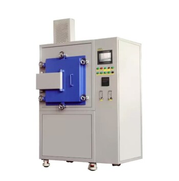
- Customer Made Versatile CVD Tube Furnace Chemical Vapor Deposition Chamber System Equipment
- Multi Heating Zones CVD Tube Furnace Machine Chemical Vapor Deposition Chamber System Equipment
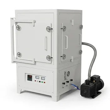
- Horizontal High Temperature Graphite Vacuum Graphitization Furnace
- Vertical High Temperature Graphite Vacuum Graphitization Furnace
- Controlled Nitrogen Inert Hydrogen Atmosphere Furnace
People Also Ask
- What is the function of a tube furnace in CVD SiC synthesis? Achieving Ultra-Pure Silicon Carbide Powders
- What is the synthesis and mechanism involved in the preparation of carbon nanotubes using CVD process? Master Controlled Growth for Your Application
- What is a CVD tube furnace? A Complete Guide to Thin-Film Deposition
- How is graphene synthesized? Choosing the Right Method for Your Application
- What is chemical vapor deposition for CNT? The Leading Method for Scalable Carbon Nanotube Synthesis