In essence, Plasma Enhanced Chemical Vapor Deposition (PECVD) is a critical manufacturing process used to deposit high-quality thin films at significantly lower temperatures than traditional methods. Its primary applications are in the fabrication of semiconductor devices, the synthesis of advanced nanomaterials like carbon nanotubes, and the creation of protective or optical coatings on heat-sensitive substrates.
The fundamental advantage of PECVD is its use of an energized plasma, rather than high heat, to drive the chemical reactions needed for film deposition. This ability to operate at low temperatures unlocks the use of substrates and device architectures that would be damaged or destroyed by conventional high-temperature processes.
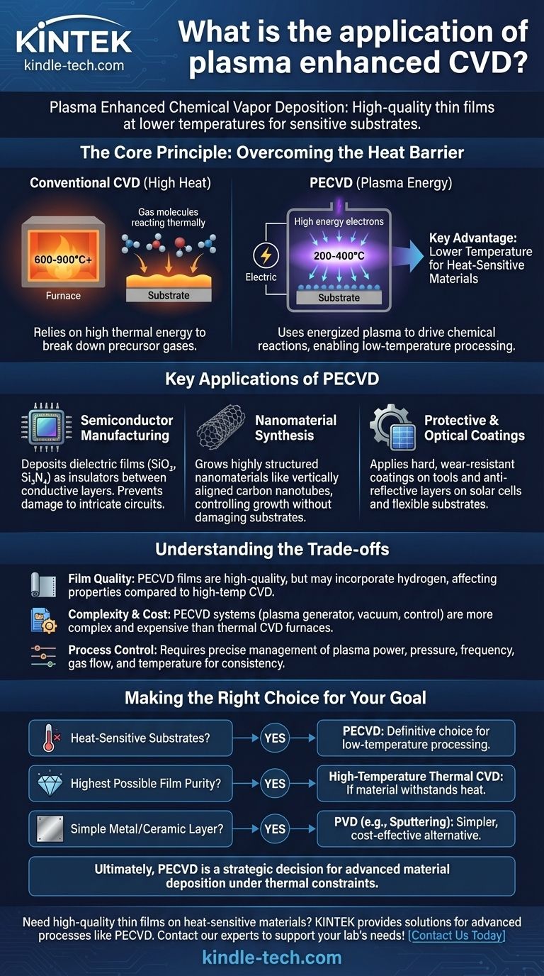
The Core Principle: Overcoming the Heat Barrier
Traditional Chemical Vapor Deposition (CVD) is like baking a cake—it relies on high heat to cause the ingredients (precursor gases) to react and form a solid layer on a surface. PECVD, however, finds a different way to supply that energy.
How Conventional CVD Works
In a standard thermal CVD process, precursor gases are introduced into a high-temperature furnace. The thermal energy breaks down these gas molecules, which then react and deposit as a solid thin film on a substrate. This often requires temperatures of 600-900°C or higher.
How PECVD Changes the Equation
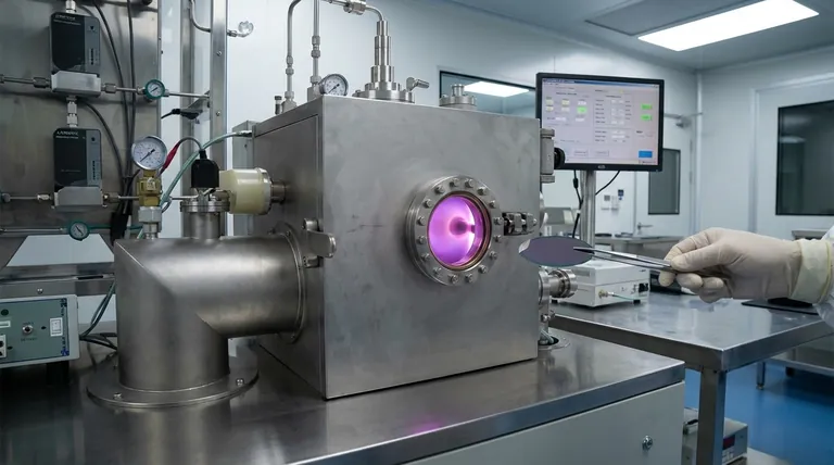
PECVD uses an electric field (often radio frequency or microwave) to ionize the precursor gases, creating a plasma. This plasma is a high-energy state of matter containing ions, electrons, and neutral particles.
The high-energy electrons in the plasma collide with gas molecules, breaking them down into reactive radicals. These radicals are highly unstable and readily deposit onto a nearby substrate, even at much lower temperatures—typically 200-400°C.
The Key Advantage: Lower Temperature
This lower processing temperature is the single most important feature of PECVD. It allows for the deposition of films on materials that cannot withstand the intense heat of thermal CVD, such as plastics, polymers, or complex integrated circuits that already have sensitive metallic layers.
Key Applications of PECVD
The low-temperature capability of PECVD makes it indispensable in several high-technology fields.
Semiconductor Manufacturing
PECVD is a workhorse in fabricating microchips. It is used to deposit dielectric films, like silicon dioxide (SiO₂) and silicon nitride (Si₃N₄), which act as insulators between conductive layers.
Depositing these films at low temperatures prevents damage to the intricate, previously fabricated metallic wiring and transistor structures on the silicon wafer. It is also used for specialized films, such as silicon carbide (SiC), on silicon substrates.
Nanomaterial Synthesis
The process is frequently used to grow highly structured nanomaterials. A prime example is the growth of vertically aligned carbon nanotubes.
The plasma helps control the growth direction and structure of the nanotubes at temperatures that do not damage the catalyst particles or the underlying substrate, enabling their use in advanced electronics and sensors.
Protective and Photovoltaic Coatings
PECVD is ideal for applying functional coatings to finished products. This includes hard, wear-resistant coatings on cutting tools and anti-reflective coatings on solar cells.
For thin-film solar cells, PECVD can deposit the active photovoltaic materials or passivation layers without subjecting the large glass or flexible substrate to damaging thermal stress.
Understanding the Trade-offs
While powerful, PECVD is not a universal solution. It involves specific trade-offs compared to other deposition methods.
Film Quality vs. Temperature
While PECVD films are high-quality, the highest-purity and most crystalline films are often produced by high-temperature thermal CVD. PECVD films can sometimes have hydrogen atoms from the precursor gases incorporated into them, which can affect electrical or optical properties.
Equipment Complexity and Cost
A PECVD system, with its required plasma generator, vacuum chamber, and control electronics, is significantly more complex and expensive than a simple furnace used for thermal CVD.
Process Control
Managing a PECVD process involves more variables than thermal CVD. In addition to gas flow and temperature, engineers must precisely control plasma power, pressure, and frequency to achieve consistent and repeatable film properties.
Making the Right Choice for Your Goal
Selecting a deposition method depends entirely on the constraints and desired outcome of your specific application.
- If your primary focus is depositing on heat-sensitive substrates like polymers or completed integrated circuits: PECVD is the definitive choice due to its low-temperature processing.
- If your primary focus is achieving the highest possible film purity and crystalline density for a robust substrate: High-temperature thermal CVD may be superior, provided your material can withstand the heat.
- If your goal is to deposit a simple metal or ceramic layer where line-of-sight deposition is acceptable: Physical Vapor Deposition (PVD) methods like sputtering can often be a simpler and more cost-effective alternative.
Ultimately, selecting PECVD is a strategic decision to enable advanced material deposition where thermal constraints make conventional methods impractical.
Summary Table:
| Application Area | Key Use Cases | PECVD Advantage |
|---|---|---|
| Semiconductor Manufacturing | Deposition of dielectric films (SiO₂, Si₃N₄) | Prevents damage to sensitive pre-fabricated circuits |
| Nanomaterial Synthesis | Growth of carbon nanotubes and structured materials | Controlled growth at low temperatures |
| Protective & Optical Coatings | Hard coatings, anti-reflective layers for solar cells | Coats heat-sensitive substrates like plastics and glass |
Need to deposit high-quality thin films on heat-sensitive materials? KINTEK specializes in lab equipment and consumables, providing solutions for advanced processes like PECVD. Our expertise can help you enhance your semiconductor, nanomaterial, or coating research and production. Contact our experts today to discuss how we can support your laboratory's specific needs!
Visual Guide
Related Products
- RF PECVD System Radio Frequency Plasma-Enhanced Chemical Vapor Deposition RF PECVD
- Chemical Vapor Deposition CVD Equipment System Chamber Slide PECVD Tube Furnace with Liquid Gasifier PECVD Machine
- Inclined Rotary Plasma Enhanced Chemical Vapor Deposition PECVD Equipment Tube Furnace Machine
- Inclined Rotary Plasma Enhanced Chemical Vapor Deposition PECVD Equipment Tube Furnace Machine
- Microwave Plasma Chemical Vapor Deposition MPCVD Machine System Reactor for Lab and Diamond Growth
People Also Ask
- What is an example of PECVD? RF-PECVD for High-Quality Thin Film Deposition
- Why is a Matching Network Indispensable in RF-PECVD for Siloxane Films? Ensure Stable Plasma and Uniform Deposition
- What is plasma enhanced chemical vapour deposition process? Unlock Low-Temperature, High-Quality Thin Films
- What is the role of RF-PECVD in VFG preparation? Mastering Vertical Growth and Surface Functionality
- What is plasma enhanced chemical vapour deposition PECVD used for? Enable Low-Temp Thin Films for Electronics & Solar


