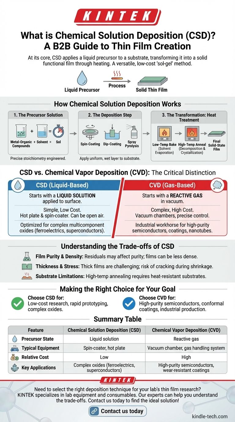
At its core, Chemical Solution Deposition (CSD) is a method for creating thin films by applying a liquid chemical precursor onto a substrate and then heating it. This process transforms the liquid into a solid, functional layer. It is a versatile, low-cost alternative to more complex vacuum-based techniques and is often referred to as the "sol-gel" method.
The defining characteristic of Chemical Solution Deposition is its use of a liquid solution as the starting material. This makes it fundamentally different from vapor-based methods and is the key to its advantages in cost and simplicity.
How Chemical Solution Deposition Works
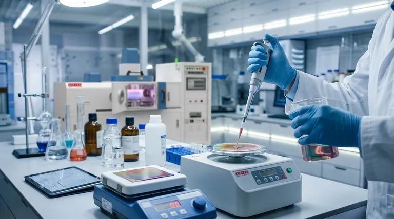
CSD is a multi-step process that starts with chemistry in a beaker and ends with a solid film on a surface. The general workflow is straightforward and adaptable.
The Precursor Solution
The process begins by dissolving metal-organic compounds in a solvent to create a liquid precursor, often called a "sol." This solution is engineered to have the precise elemental ratio (stoichiometry) required for the final film.
The Deposition Step
The liquid precursor is applied to a substrate, which is the base material for the film. Common application methods include spin-coating, dip-coating, or spray pyrolysis. The goal is to create a uniform, wet layer across the surface.
The Transformation: Heat Treatment
After deposition, the coated substrate undergoes a series of heat treatments. A low-temperature bake first drives off the solvent. A subsequent high-temperature anneal then decomposes the remaining organic compounds and crystallizes the material into the desired solid-state phase.
The Critical Distinction: CSD vs. Chemical Vapor Deposition (CVD)
The provided references confuse CSD with Chemical Vapor Deposition (CVD), a common point of misunderstanding. While both create thin films, their principles are entirely different.
The Precursor State: Liquid vs. Gas
This is the most fundamental difference. CSD starts with a liquid solution applied directly to the surface. In contrast, CVD starts with a reactive gas that is introduced into a vacuum chamber where it reacts on the substrate's surface to form the film.
Process Complexity and Cost
CSD is valued for its simplicity and low cost. It often requires little more than a hot plate and a spin-coater, and can even be done in open air. CVD is a highly complex process requiring expensive vacuum chambers, gas handling systems, and precise temperature control, demanding a high level of operator skill.
Typical Applications
The two methods are optimized for different materials and outcomes. CSD excels at producing complex multicomponent oxide films, such as ferroelectrics and superconductors. CVD is an industrial workhorse for depositing high-purity semiconductor films, wear-resistant coatings, and materials like carbon nanotubes.
Understanding the Trade-offs of CSD
While powerful, CSD is not a universal solution. Understanding its limitations is crucial for making an informed decision.
Film Purity and Density
Because the film originates from a solvent-based precursor, residual carbon or other impurities from the liquid can sometimes be incorporated into the final film, affecting its purity. The films can also be less dense than those produced by vacuum methods.
Thickness and Stress
Achieving very thick films with CSD can be challenging. Applying too much solution at once can lead to cracking as the solvent evaporates and the material shrinks during heating. Building thickness requires multiple coating and heating cycles.
Substrate Limitations
The high-temperature annealing step required for CSD means the substrate material must be able to withstand significant heat without degrading or reacting. This limits its use with plastics or other low-melting-point materials.
Making the Right Choice for Your Goal
Selecting a deposition technique depends entirely on your project's priorities, from budget to the specific material properties you need to achieve.
- If your primary focus is low-cost research, rapid prototyping, or creating complex oxide materials: CSD is an excellent and highly accessible choice due to its simple equipment and stoichiometric control.
- If your primary focus is producing high-purity semiconductor films, conformal coatings on complex shapes, or industrial-scale production: CVD is the established and more suitable method, despite its higher cost and complexity.
Ultimately, understanding the fundamental difference between a liquid-based and a gas-based process empowers you to select the right tool for the job.
Summary Table:
| Feature | Chemical Solution Deposition (CSD) | Chemical Vapor Deposition (CVD) |
|---|---|---|
| Precursor State | Liquid solution | Reactive gas |
| Typical Equipment | Spin-coater, hot plate | Vacuum chamber, gas handling system |
| Relative Cost | Low | High |
| Key Applications | Complex oxides (ferroelectrics, superconductors) | High-purity semiconductors, wear-resistant coatings |
Need to select the right deposition technique for your lab's thin film research? KINTEK specializes in lab equipment and consumables, serving laboratory needs. Our experts can help you understand the trade-offs between CSD and other methods to optimize your process for cost, purity, and performance. Contact us today to discuss your specific application and find the ideal solution!
Visual Guide
Related Products
- Chemical Vapor Deposition CVD Equipment System Chamber Slide PECVD Tube Furnace with Liquid Gasifier PECVD Machine
- HFCVD Machine System Equipment for Drawing Die Nano-Diamond Coating
- RF PECVD System Radio Frequency Plasma-Enhanced Chemical Vapor Deposition RF PECVD
- Customer Made Versatile CVD Tube Furnace Chemical Vapor Deposition Chamber System Equipment
- Microwave Plasma Chemical Vapor Deposition MPCVD Machine System Reactor for Lab and Diamond Growth
People Also Ask
- How expensive is chemical vapor deposition? Understanding the True Cost of High-Performance Coating
- What is plasma enhanced chemical vapor deposition PECVD equipment? A Guide to Low-Temperature Thin Film Deposition
- What is the chemical vapor deposition growth process? Build Superior Thin Films from the Atom Up
- What are the advantages of chemical vapor deposition? Achieve Superior Thin Films for Your Lab
- What are the core advantages of PE-CVD in OLED encapsulation? Protect Sensitive Layers with Low-Temp Film Deposition


