At its core, Metal-Organic Chemical Vapor Deposition (MOCVD) is a specialized, high-precision type of Chemical Vapor Deposition (CVD). The fundamental difference lies in the chemical precursors used to create the thin film. MOCVD specifically uses metal-organic compounds, which enables lower process temperatures and exceptional control over the growth of complex, multi-layer crystalline structures.
The decision between MOCVD and general CVD is not about which is "better," but about aligning the tool with the task. MOCVD offers unparalleled precision for creating complex semiconductor structures, while standard CVD provides a robust, scalable, and cost-effective solution for a wider range of industrial applications.
The Fundamental Difference: Precursor Materials
To understand the two processes, you must first understand the role of the precursor. In any vapor deposition process, a precursor is a chemical compound that contains the atoms you want to deposit. When heated, this precursor decomposes and the desired atoms settle onto a substrate, forming a thin film.
How Standard CVD Works
Standard CVD is a broad category of techniques that can use a variety of precursors. These are often inorganic compounds, such as silane (SiH₄) for depositing silicon or tungsten hexafluoride (WF₆) for depositing tungsten. These precursors are typically gases or liquids/solids that must be vaporized at high temperatures to be transported to the substrate.
The MOCVD Approach: Metal-Organic Precursors
MOCVD, sometimes called OMVPE (Organometallic Vapor-Phase Epitaxy), refines this process by exclusively using metal-organic precursors. These are complex molecules where a central metal atom is bonded to organic molecules. A common example is trimethylgallium (Ga(CH₃)₃) used for depositing gallium. These precursors are often liquids that vaporize easily at low temperatures.
This specific choice of precursor is the source of all of MOCVD's unique characteristics.
Comparing Key Process Characteristics
The use of metal-organic precursors leads to significant practical differences in how the processes are run and the results they can achieve.
Operating Temperature
MOCVD systems generally operate at lower temperatures than many conventional CVD processes. Because metal-organic precursors are designed to decompose more readily, you can achieve film growth without exposing the substrate to extreme heat. This is critical when working with materials that can be damaged by high temperatures.
Deposition Control and Film Quality
This is where MOCVD truly excels. The process allows for extremely fine control over the thickness and composition of the deposited film, down to a single atomic layer. It enables the creation of abrupt interfaces—sharp, clean boundaries between different material layers—and provides excellent dopant control, which is crucial for manufacturing modern electronics.
For this reason, MOCVD is the dominant method for growing high-purity crystalline compound semiconductor films, such as those used in LEDs, laser diodes, and high-performance transistors.
Process Complexity
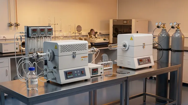
The precision of MOCVD comes at the cost of increased complexity. The systems require sophisticated handling of the liquid metal-organic precursors, precise gas flow and mixing controls, and often operate under vacuum conditions. Standard CVD systems, while diverse, can often be simpler to implement.
Understanding the Trade-offs: Cost vs. Precision
Choosing between these technologies is a classic engineering trade-off between performance requirements and economic reality.
The Case for MOCVD: High-Value Applications
MOCVD is the go-to process when the absolute highest material quality and atomic-level control are non-negotiable. Its ability to create complex, defect-free crystalline structures makes it indispensable for the optoelectronics and high-frequency electronics industries. The higher operational cost is justified by the performance of the final device.
The Case for CVD: Scalability and Simplicity
Traditional CVD methods are workhorses of industrial manufacturing. They are highly effective for depositing durable, uniform films over large areas. While they may not offer the atomic precision of MOCVD, they are more than sufficient for many applications, from hard coatings on tools to depositing common layers in silicon-based microchips. Their simplicity and lower cost make them ideal for large-scale production.
A Note on Cost and Implementation
An MOCVD reactor is a significantly more expensive piece of equipment than many standard CVD systems. The metal-organic precursors themselves are also costly and require specialized safety protocols. For a research lab or a production line with a limited budget, a simpler CVD process is often a more practical starting point.
Making the Right Choice for Your Application
Your final decision must be driven by the specific requirements of your film and the economic constraints of your project.
- If your primary focus is high-performance optoelectronics (LEDs, lasers) or compound semiconductors: MOCVD is the necessary choice for achieving the required crystalline quality and complex layer structures.
- If your primary focus is large-scale deposition of simpler films (e.g., silicon dioxide, tungsten, hard coatings): A standard CVD method will provide the required performance at a much lower cost and higher throughput.
- If your primary focus is research on a limited budget for non-critical films: The lower cost and relative simplicity of a standard CVD system make it a more practical and accessible option.
Ultimately, choosing the right deposition technique requires a clear understanding of your material, performance targets, and production scale.
Summary Table:
| Characteristic | Standard CVD | MOCVD |
|---|---|---|
| Primary Precursors | Inorganic gases/vapors | Metal-organic compounds |
| Operating Temperature | Generally higher | Lower |
| Primary Strength | Scalability, cost-effectiveness | Atomic-level precision, crystalline quality |
| Typical Applications | Hard coatings, silicon-based microchips | LEDs, laser diodes, compound semiconductors |
Ready to Choose the Right Deposition System for Your Lab?
KINTEK specializes in lab equipment and consumables, serving laboratory needs. Whether you're developing next-generation optoelectronics or need reliable, scalable thin-film deposition, our experts can help you select the perfect CVD or MOCVD solution for your specific application and budget.
We provide:
- Tailored equipment recommendations based on your material and performance requirements
- Comprehensive support for research labs and production facilities
- Cost-effective solutions that balance precision with scalability
Contact us today to discuss your thin film deposition needs and discover how KINTEK can enhance your laboratory's capabilities!
Visual Guide

Related Products
- CVD Diamond Dressing Tools for Precision Applications
- Multi Heating Zones CVD Tube Furnace Machine Chemical Vapor Deposition Chamber System Equipment
- CVD Diamond Domes for Industrial and Scientific Applications
- CVD Diamond for Thermal Management Applications
- Chemical Vapor Deposition CVD Equipment System Chamber Slide PECVD Tube Furnace with Liquid Gasifier PECVD Machine
People Also Ask
- What color diamonds are CVD? Understanding the Process from Brown Tint to Colorless Beauty
- What are the raw materials for CVD diamonds? A seed, a gas, and the science of crystal growth.
- Does the chemical vapor deposition be used for diamonds? Yes, for Growing High-Purity Lab Diamonds
- What are the disadvantages of CVD diamonds? Understanding the trade-offs for your purchase.
- How do you identify a CVD diamond? The Definitive Guide to Lab-Grown Diamond Verification
