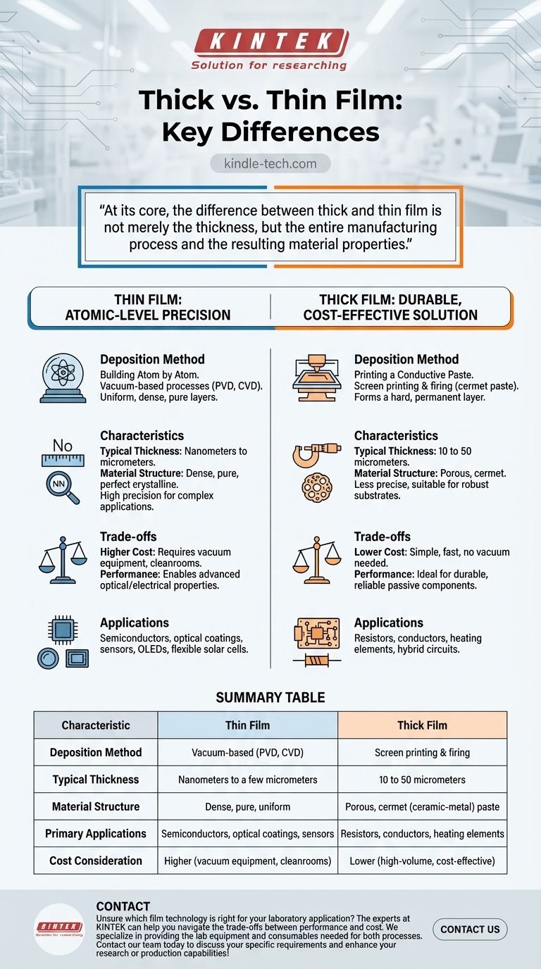
At its core, the difference between thick and thin film is not merely the thickness, but the entire manufacturing process and the resulting material properties. A thin film is a layer of material, often just atoms or molecules thick, deposited in a vacuum. In contrast, a thick film is a paste-like ink that is printed onto a surface and then fired in a furnace.
The choice between thin and thick film technology represents a fundamental trade-off. Thin film offers atomic-level precision for complex optical and semiconductor applications, while thick film provides a durable, cost-effective solution for simpler electronic components.
The Defining Factor: Deposition Method
The most important distinction arises from how each film is created. The process dictates the film's structure, purity, and ultimate capabilities.
Thin Film: Building Atom by Atom
Thin films are created using deposition processes that build the layer one atom or molecule at a time. Methods like Physical Vapor Deposition (PVD) or Chemical Vapor Deposition (CVD) occur in a vacuum.
This atomic-level control results in films that are extremely uniform, dense, and pure. They can range from a single layer of atoms (fractions of a nanometer) to several micrometers thick.
Thick Film: Printing a Conductive Paste
Thick films are made using a process similar to screen printing. A cermet paste—a mixture of metal, glass, and organic binders—is squeezed through a mesh screen onto a substrate.
After printing, the substrate is fired in a high-temperature furnace. This burns off the organic binder and fuses the particles together, forming a hard, permanent layer that is typically 10 to 50 micrometers thick.
Comparing Core Characteristics
The different manufacturing methods lead to vastly different physical properties and performance characteristics.
Thickness and Precision
Thin films offer exceptional precision, with thickness controlled down to the nanometer. This is essential for applications like optical coatings and semiconductors.
Thick films are inherently less precise. Their thickness is orders of magnitude greater and has a much lower degree of control, which is perfectly acceptable for their intended applications.
Material Purity and Density
Because they are deposited in a vacuum, thin films are highly pure and dense, with an almost perfect crystalline structure. This is critical for achieving specific electrical and optical properties.
Thick films are naturally porous. The firing process sinters particles together but leaves microscopic voids, resulting in a less dense material compared to its thin-film counterpart.
Substrate Compatibility
Thin film deposition often requires very smooth, clean substrates (like silicon wafers or glass) and must be done in a highly controlled cleanroom environment.
Thick film technology is far more forgiving. It is commonly used on robust ceramic substrates like alumina and can tolerate less pristine environments, which lowers production costs.
Understanding the Trade-offs: Cost vs. Performance
Your choice between these technologies is almost always a decision between manufacturing cost and performance requirements.
The Cost Equation
Thick film processing is relatively simple, fast, and does not require a vacuum. This makes it significantly cheaper and ideal for high-volume manufacturing of components like resistors or hybrid circuits.
Thin film deposition requires expensive vacuum equipment, cleanrooms, and longer processing times. This higher cost is justified by the unique capabilities it enables.
The Performance Ceiling
Thick film technology excels at creating durable, reliable passive components. However, its porosity and lack of precision limit its use in high-frequency or high-precision applications.
Thin film technology opens the door to advanced applications. As the references note, it enables materials that are anti-reflective, optically transparent yet electrically conductive, and suitable for semiconductors, flexible solar cells, and OLEDs.
Making the Right Choice for Your Goal
To select the correct technology, you must align its fundamental characteristics with your project's primary objective.
- If your primary focus is precision, advanced optical/electrical properties, or miniaturization: Thin film technology is the necessary choice for creating high-performance semiconductors, sensors, and optical coatings.
- If your primary focus is durability, cost-effective production, and simpler electronic functions: Thick film technology is the more practical and economical solution for components like resistors, conductors, and heating elements on ceramic.
Ultimately, understanding the link between the manufacturing process and the final performance is the key to making an informed decision.
Summary Table:
| Characteristic | Thin Film | Thick Film |
|---|---|---|
| Deposition Method | Vacuum-based (PVD, CVD) | Screen printing & firing |
| Typical Thickness | Nanometers to a few micrometers | 10 to 50 micrometers |
| Material Structure | Dense, pure, uniform | Porous, cermet (ceramic-metal) paste |
| Primary Applications | Semiconductors, optical coatings, sensors | Resistors, conductors, heating elements |
| Cost Consideration | Higher (vacuum equipment, cleanrooms) | Lower (high-volume, cost-effective) |
Unsure which film technology is right for your laboratory application? The experts at KINTEK can help you navigate the trade-offs between performance and cost. We specialize in providing the lab equipment and consumables needed for both thin and thick film processes. Contact our team today to discuss your specific requirements and enhance your research or production capabilities!
Visual Guide
Related Products
- RF PECVD System Radio Frequency Plasma-Enhanced Chemical Vapor Deposition RF PECVD
- Aluminized Ceramic Evaporation Boat for Thin Film Deposition
- Hemispherical Bottom Tungsten Molybdenum Evaporation Boat
- Vacuum Hot Press Furnace Machine for Lamination and Heating
- Lab Plastic PVC Calender Stretch Film Casting Machine for Film Testing
People Also Ask
- How are PECVD and CVD different? A Guide to Choosing the Right Thin-Film Deposition Process
- Why is PECVD environment friendly? Understanding the Eco-Friendly Benefits of Plasma-Enhanced Coating
- What is plasma activated chemical vapour deposition method? A Low-Temperature Solution for Advanced Coatings
- What are the advantages of PECVD? Enable Low-Temperature, High-Quality Thin-Film Deposition
- What is the principle of plasma enhanced chemical vapor deposition? Achieve Low-Temperature Thin Film Deposition