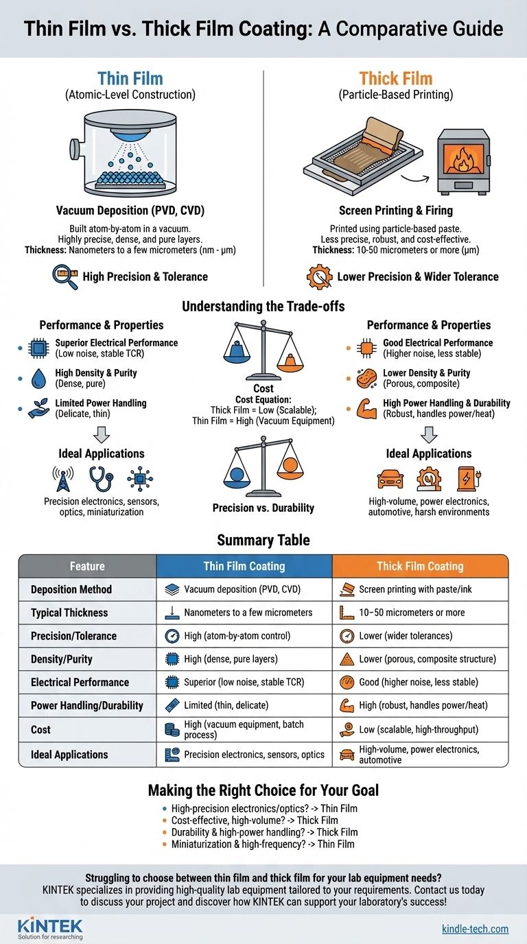
At its core, the difference between thin film and thick film coatings is not just their physical thickness, but the fundamental process used to create them. Thin films are built atom-by-atom in a vacuum, resulting in highly precise and pure layers. Thick films are printed using a particle-based paste or ink, creating a less precise but more robust and cost-effective coating.
The choice is a classic engineering trade-off. Thin film technology offers unparalleled precision and electrical performance for sensitive applications, while thick film technology provides durability and low-cost manufacturing for high-volume or high-power components.
The Defining Factor: Deposition Method
The primary distinction between thin and thick film comes from how they are applied to a substrate. This foundational difference in process dictates nearly every other property, from density and purity to cost and performance.
Thin Film: Atomic-Level Construction
Thin films are created using deposition processes that occur in a vacuum. These methods build the film layer by layer on a molecular or atomic scale.
The most common methods are Physical Vapor Deposition (PVD) and Chemical Vapor Deposition (CVD). In these processes, material is vaporized and then condenses onto the substrate, forming an extremely uniform, dense, and pure film. This layer is typically between a few nanometers (nm) and a few micrometers (µm) thick.
Thick Film: Particle-Based Printing
Thick films are most often applied using a screen-printing process, similar to how a graphic is printed on a t-shirt. A "paste" or "ink"—a mixture of the functional material (like a metal), a glass frit binder, and an organic solvent—is pushed through a mesh screen onto the substrate.
The part is then fired in a furnace. The organic solvent burns off, and the glass frit melts to bind the functional particles together and to the substrate. The resulting film is much thicker (typically 10-50 µm or more), more porous, and less pure than a thin film.
Key Differences in Performance and Properties
The deposition method directly impacts the final characteristics of the coating. Understanding these differences is crucial for selecting the right technology for your application.
Precision and Tolerance
Thin films offer exceptional precision. Because they are deposited atom-by-atom, their thickness is highly controllable, and features can be patterned with photolithography to create extremely fine lines. This results in components, like resistors, with very tight tolerances.
Thick films are inherently less precise. The screen-printing process and the particle-based nature of the paste lead to greater variation in thickness and line definition. Tolerances are wider, and post-processing steps like laser trimming are often required to achieve specific values.
Purity and Density
Thin films are almost completely dense and have very high purity. The vacuum environment prevents contamination, resulting in a film with properties very close to the bulk material.
Thick films are porous by nature. The binder material that holds the functional particles together creates a composite structure that is less dense and whose properties are a combination of all the materials in the paste.
Electrical Performance
For demanding electronic applications, thin film is superior. Its purity and uniform structure lead to lower electrical noise, better high-frequency performance, and a more stable temperature coefficient of resistance (TCR).
Thick film components are workhorses for general-purpose electronics. While their performance is excellent for many applications, the impurities and porous structure result in higher noise and less stability compared to thin film counterparts.
Power Handling and Durability
The greater physical mass of a thick film allows it to handle significantly more power and dissipate heat more effectively. These coatings are generally more mechanically robust and resistant to environmental stress and power surges.
Thin films, being incredibly thin, have limited power-handling capability and can be more susceptible to physical damage if not properly protected.
Understanding the Trade-offs
Neither technology is universally better; they are optimized for different goals. The most significant trade-off is between manufacturing cost and performance precision.
The Cost Equation
Thick film manufacturing is a relatively simple, high-throughput process. Screen printing is fast, inexpensive, and highly scalable, making it the dominant choice for mass-produced components like chip resistors and hybrid integrated circuits.
Thin film deposition requires sophisticated vacuum equipment and is a much slower, batch-oriented process. The capital investment and operational costs are significantly higher, reserving its use for applications where its superior performance is a necessity.
Application Environment
Thick films excel in harsh automotive, industrial, and power electronics environments due to their inherent ruggedness.
Thin films are the standard in applications where precision, miniaturization, and high-frequency performance are critical, such as in telecommunications, medical devices, and high-precision sensors.
Making the Right Choice for Your Goal
Your application's primary requirement should guide your decision between thin and thick film technology.
- If your primary focus is high-precision electronics or optics: Choose thin film for its superior uniformity, tight tolerances, and excellent electrical properties.
- If your primary focus is cost-effective, high-volume production: Choose thick film for its low manufacturing cost and rapid, scalable screen-printing process.
- If your primary focus is durability and high-power handling: Choose thick film for its physical robustness and ability to dissipate heat and manage higher electrical loads.
- If your primary focus is miniaturization and high-frequency performance: Choose thin film for its ability to create precise, small-scale features with outstanding signal integrity.
Ultimately, selecting the correct film technology is about aligning the process capabilities with your specific performance targets and economic constraints.
Summary Table:
| Feature | Thin Film Coating | Thick Film Coating |
|---|---|---|
| Deposition Method | Vacuum deposition (PVD, CVD) | Screen printing with paste/ink |
| Typical Thickness | Nanometers to a few micrometers | 10–50 micrometers or more |
| Precision/Tolerance | High (atom-by-atom control) | Lower (wider tolerances) |
| Density/Purity | High (dense, pure layers) | Lower (porous, composite structure) |
| Electrical Performance | Superior (low noise, stable TCR) | Good (higher noise, less stable) |
| Power Handling/Durability | Limited (thin, delicate) | High (robust, handles power/heat) |
| Cost | High (vacuum equipment, batch process) | Low (scalable, high-throughput) |
| Ideal Applications | Precision electronics, sensors, optics | High-volume, power electronics, automotive |
Struggling to choose between thin film and thick film for your lab equipment needs? KINTEK specializes in providing high-quality lab equipment and consumables tailored to your specific coating requirements. Whether you need the precision of thin film deposition or the durability of thick film processes, our experts can help you select the right solution to enhance your lab's efficiency and performance. Contact us today to discuss your project and discover how KINTEK can support your laboratory's success!
Visual Guide