At its core, Chemical Vapor Deposition (CVD) is a growth mechanism where volatile chemical precursors react in a controlled environment to produce a high-purity solid film on a substrate. The process involves transporting these precursor gases to the substrate surface, where a chemical reaction, typically activated by heat, causes them to decompose and deposit the desired material layer by layer.
The fundamental mechanism of CVD is not a single action, but a sequence of events. It is the controlled transformation of gas-phase chemicals into a solid film through a series of transport and surface-reaction steps, allowing for atomic-level control over material growth.
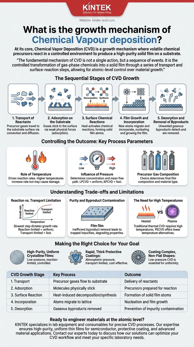
The Sequential Stages of CVD Growth
Understanding CVD growth requires breaking it down into a series of distinct physical and chemical steps. The quality and properties of the final film depend on which of these stages is the rate-limiting factor.
Stage 1: Transport of Reactants
Precursor gases are introduced into a reaction chamber. They must then travel from the gas inlet to the surface of the workpiece, which is known as the substrate.
This movement occurs through a combination of convection (the bulk flow of gas) and diffusion (the random motion of molecules driven by a concentration gradient).
Stage 2: Adsorption on the Substrate
Once the gas molecules reach the substrate, they must stick to the surface. This process is called adsorption.
The molecules are not yet chemically bonded but are held on the surface by weak physical forces, ready for the next stage.
Stage 3: Surface Chemical Reactions
This is the heart of the CVD process. With energy supplied, typically from heating the substrate, the adsorbed precursor molecules undergo chemical reactions.
These reactions can be a decomposition (a single molecule breaking down) or a synthesis (multiple molecules reacting together) to form the atoms of the desired solid film.
Stage 4: Film Growth and Incorporation
The newly formed solid atoms or molecules must find their place on the surface. They may migrate across the surface until they find an energetically favorable site, such as the edge of a crystal lattice.
This incorporation leads to the nucleation and subsequent growth of the thin film. The ability to control this step allows for the creation of highly ordered, crystalline materials like the graphene or diamond films mentioned in advanced applications.
Stage 5: Desorption and Removal of Byproducts
The chemical reactions that form the solid film also create unwanted gaseous byproducts.
These byproduct molecules must detach from the surface (desorption) and be transported away by the gas flow. Efficient removal is critical to prevent them from becoming incorporated into the film as impurities.
Controlling the Outcome: Key Process Parameters
The final film's characteristics—its purity, thickness, crystal structure, and uniformity—are dictated by fine-tuning the deposition parameters, which directly influence the growth mechanism.
The Role of Temperature
Temperature is the primary driver of the surface chemical reactions. Higher temperatures increase the reaction rate, but excessive heat can damage the substrate or lead to undesirable gas-phase reactions before the precursors reach the surface.
The Influence of Pressure
The pressure inside the chamber determines the concentration of precursor gases and the mean free path—the average distance a molecule travels before colliding with another.
Low-Pressure CVD (LPCVD) results in a longer mean free path, leading to highly uniform coatings even on complex shapes, as the growth is limited by the surface reaction rate. Atmospheric Pressure CVD (APCVD) allows for much faster deposition but can result in less uniformity.
Precursor Gas Composition
The choice of gases and their flow rates directly determine the chemical composition of the final film. By introducing different precursors, one can create a wide variety of materials, including metals, ceramics, and complex alloys.
Understanding the Trade-offs and Limitations
While powerful, the CVD process involves critical trade-offs that every practitioner must manage.
Reaction vs. Transport Limitation
The overall growth rate is determined by the slowest step in the sequence. If growth is reaction-limited, the film is often very uniform because the chemical reaction rate is the same everywhere on the surface. If it is transport-limited, the film grows fastest where the reactants are most plentiful, which can lead to non-uniformity.
Purity and Byproduct Contamination
If byproducts are not removed efficiently, they can become trapped in the growing film. This is a primary source of impurities that can degrade the material's electronic or optical properties.
The Need for High Temperatures
Traditional thermal CVD requires high temperatures, which restricts its use to substrates that can withstand the heat. This limitation has driven the development of alternative methods like Plasma-Enhanced CVD (PECVD), which uses a plasma to provide the reaction energy, allowing for deposition at much lower temperatures.
Making the Right Choice for Your Goal
Understanding the growth mechanism allows you to tailor the CVD process to a specific outcome.
- If your primary focus is high-purity, uniform crystalline films (e.g., for semiconductors): You should use a low-pressure, reaction-limited process where temperature and gas flow are meticulously controlled.
- If your primary focus is rapid, thick protective coatings: An atmospheric-pressure, transport-limited process may be more cost-effective, even if it sacrifices some uniformity.
- If your primary focus is coating complex, non-flat shapes: A low-pressure CVD process is essential to ensure the precursor gases can uniformly reach and react on all surfaces.
Mastering these fundamental stages empowers you to move beyond simply using a process to truly engineering materials at the atomic scale.
Summary Table:
| CVD Growth Stage | Key Process | Outcome |
|---|---|---|
| 1. Transport | Precursor gases flow to substrate | Delivery of reactants to surface |
| 2. Adsorption | Molecules physically stick to surface | Precursors prepared for reaction |
| 3. Surface Reaction | Heat-induced decomposition/synthesis | Formation of solid film atoms |
| 4. Incorporation | Atoms migrate to crystal lattice sites | Nucleation and film growth |
| 5. Desorption | Gaseous byproducts removed from surface | Prevention of impurity contamination |
Ready to engineer materials at the atomic level? KINTEK specializes in lab equipment and consumables for precise CVD processes. Our expertise ensures you achieve high-purity, uniform thin films for semiconductor, protective coating, and advanced material applications.
Contact our experts today to discuss how our solutions can optimize your CVD workflow and meet your specific laboratory needs.
Visual Guide
Related Products
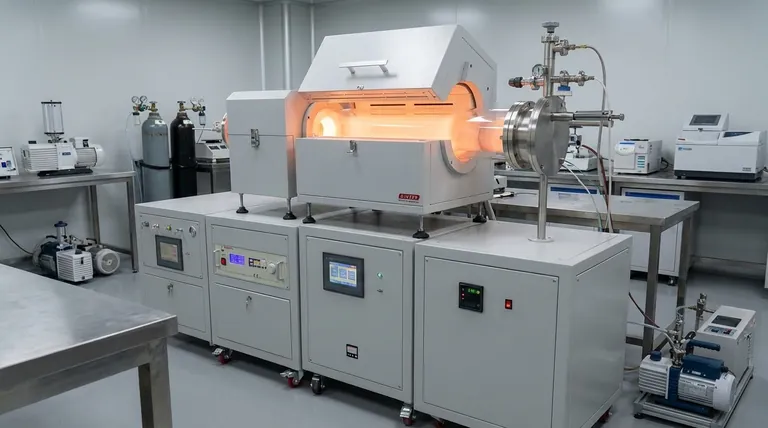
- Chemical Vapor Deposition CVD Equipment System Chamber Slide PECVD Tube Furnace with Liquid Gasifier PECVD Machine
- RF PECVD System Radio Frequency Plasma-Enhanced Chemical Vapor Deposition RF PECVD
- Microwave Plasma Chemical Vapor Deposition MPCVD Machine System Reactor for Lab and Diamond Growth
- Customer Made Versatile CVD Tube Furnace Chemical Vapor Deposition Chamber System Equipment
- 915MHz MPCVD Diamond Machine Microwave Plasma Chemical Vapor Deposition System Reactor
People Also Ask
- What is the chemical vapor deposition growth process? Build Superior Thin Films from the Atom Up
- What happens during deposition chemistry? Building Thin Films from Gaseous Precursors
- How are carbon nanotubes grown? Master Scalable Production with Chemical Vapor Deposition
- What are the advantages of chemical vapor deposition? Achieve Superior Thin Films for Your Lab
- What types of substrates are used in CVD to facilitate graphene films? Optimize Graphene Growth with the Right Catalyst


