In short, deposition precipitation is a general term for any process where a solid material is formed, or "precipitated," onto a surface from a surrounding medium like a gas, plasma, or solution. It is more commonly known as thin film deposition, a foundational process in manufacturing electronics, optics, and advanced materials. The core principle involves generating atoms or molecules of a desired material and precisely controlling their condensation or reaction onto a target object, called a substrate.
At its core, every deposition process follows the same fundamental sequence: a material is converted into a mobile state (like a vapor), transported to a surface, and then converted back into a solid film under controlled conditions. The specific method used to achieve this sequence defines the technique and its unique capabilities.
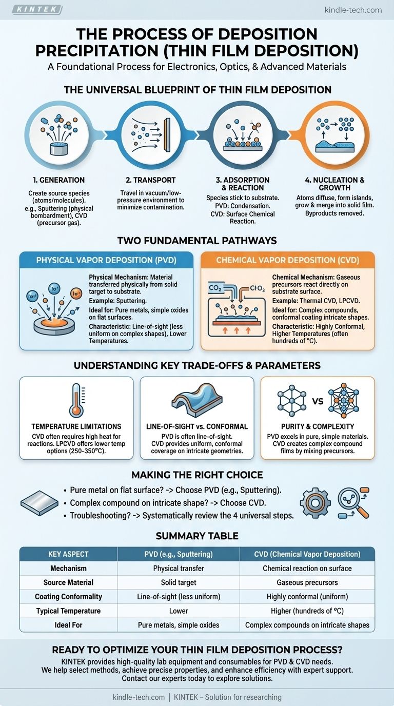
The Universal Blueprint of Thin Film Deposition
While specific techniques vary, nearly all deposition processes can be broken down into four essential, chronological steps. Understanding this universal blueprint is the key to demystifying how thin films are made.
Step 1: Generation of the Deposition Species
The first step is to create a source of atoms or molecules that will form the film. This is the primary distinction between different deposition families.
For example, in sputtering, a physical process, high-energy ions (like argon) bombard a solid "target" of the desired material, physically knocking atoms loose and ejecting them into the chamber.
In Chemical Vapor Deposition (CVD), the source is a precursor gas. This volatile compound is introduced into the chamber, carrying the necessary elements in a gaseous state.
Step 2: Transport to the Substrate
Once generated, these atoms or molecules must travel from their source to the substrate where the film will be grown.
This transport typically occurs in a vacuum or controlled low-pressure environment. This minimizes contamination from unwanted background gases and controls the path the species take to the substrate.
Step 3: Adsorption and Surface Reaction
When the species arrive at the substrate, they must stick to the surface in a process called adsorption.
In purely physical processes, this is essentially condensation. In chemical processes like CVD, this is a critical stage where the adsorbed precursor molecules react, often triggered by the high temperature of the substrate.
Step 4: Nucleation, Growth, and Byproduct Removal
The adsorbed atoms don't form a perfect film instantly. They diffuse across the surface, find stable sites, and form small islands in a process called nucleation.
These islands then grow and merge to form a continuous, solid film. In chemical processes, this step also involves the desorption of any gaseous byproducts from the surface reactions, which are then pumped out of the chamber.
Two Fundamental Pathways: Physical vs. Chemical
The four steps above are universal, but the methods used to achieve them generally fall into two major categories.
Physical Vapor Deposition (PVD)
PVD techniques use physical mechanisms to transfer material. Sputtering is a classic example. The material being deposited starts as a solid, is converted into a vapor through physical means (bombardment), and condenses back into a solid on the substrate.
Chemical Vapor Deposition (CVD)
CVD techniques use chemistry to build the film. Gaseous precursors undergo chemical reactions directly on the substrate's surface, leaving behind a solid film as a nonvolatile product. The final film material is different from the starting gases.
Understanding the Trade-offs and Key Parameters
The choice between deposition methods is driven by the desired outcome, and success depends on precise control over several variables. There is no single "best" method, only the right one for a specific application.
Temperature Limitations
CVD processes often require high temperatures (hundreds of degrees Celsius) to drive the necessary chemical reactions. This can make them unsuitable for substrates that are sensitive to heat. Low-Pressure CVD (LPCVD) is one variation that operates at lower temperatures (250-350°C), making it more economical and versatile.
Line-of-Sight vs. Conformal Coatings
Many PVD processes like sputtering are "line-of-sight," meaning they coat surfaces that are directly exposed to the source. This makes it difficult to evenly coat complex, three-dimensional shapes. CVD processes, which rely on a gas, can often produce highly conformal coatings that uniformly cover intricate geometries.
Purity and Complexity
PVD is often excellent for depositing very pure, simple materials like metals or basic oxides. CVD excels at creating complex compound materials (like silicon nitride or titanium carbide) by carefully mixing different precursor gases.
Making the Right Choice for Your Goal
Understanding the core process allows you to evaluate which technique is suitable for a given objective.
- If your primary focus is depositing a pure metal onto a flat surface: A physical process like sputtering is often a direct and effective choice.
- If your primary focus is creating a uniform, complex compound film on an intricate shape: A chemical process like CVD is likely the superior approach.
- If you are troubleshooting a deposition process: Systematically review the four universal steps—generation, transport, adsorption/reaction, and growth—to isolate the potential source of the problem.
By grasping these fundamental principles, you can effectively analyze, compare, and control virtually any thin film deposition process.
Summary Table:
| Key Aspect | PVD (e.g., Sputtering) | CVD (Chemical Vapor Deposition) |
|---|---|---|
| Mechanism | Physical transfer (e.g., bombardment) | Chemical reaction on substrate surface |
| Source Material | Solid target | Gaseous precursors |
| Coating Conformality | Line-of-sight (less uniform on complex shapes) | Highly conformal (uniform on complex geometries) |
| Typical Temperature | Lower | Higher (often hundreds of °C) |
| Ideal For | Pure metals, simple oxides on flat surfaces | Complex compounds (e.g., silicon nitride) on intricate shapes |
Ready to Optimize Your Thin Film Deposition Process?
Whether you are developing advanced electronics, optical coatings, or specialized materials, choosing the right deposition technique is critical for performance and yield. KINTEK specializes in providing high-quality lab equipment and consumables tailored to your specific deposition needs—from sputtering targets for PVD to precursor gases for CVD.
We help you:
- Select the ideal method (PVD or CVD) for your substrate and application.
- Achieve precise film properties, from purity to conformality.
- Enhance process efficiency with reliable equipment and expert support.
Let’s discuss your project requirements. Contact our experts today to explore how KINTEK’s solutions can advance your research or production goals.
Visual Guide
Related Products
- Aluminized Ceramic Evaporation Boat for Thin Film Deposition
- Tungsten Evaporation Boat for Thin Film Deposition
- Electron Beam Evaporation Coating Oxygen-Free Copper Crucible and Evaporation Boat
- Molybdenum Tungsten Tantalum Evaporation Boat for High Temperature Applications
- Vacuum Hot Press Furnace Machine for Lamination and Heating
People Also Ask
- Why is an alumina boat and Ti3AlC2 powder bed necessary for Ti2AlC sintering? Protect MAX Phase Purity
- What is the widely used boat made of in thermal evaporation? Choosing the Right Material for High-Purity Deposition
- What is the chemical method for thin film deposition? Build Films from the Molecular Level Up
- What are the alternatives to sputtering? Choose the Right Thin Film Deposition Method
- What is thin film deposition? Unlock Advanced Surface Engineering for Your Materials


