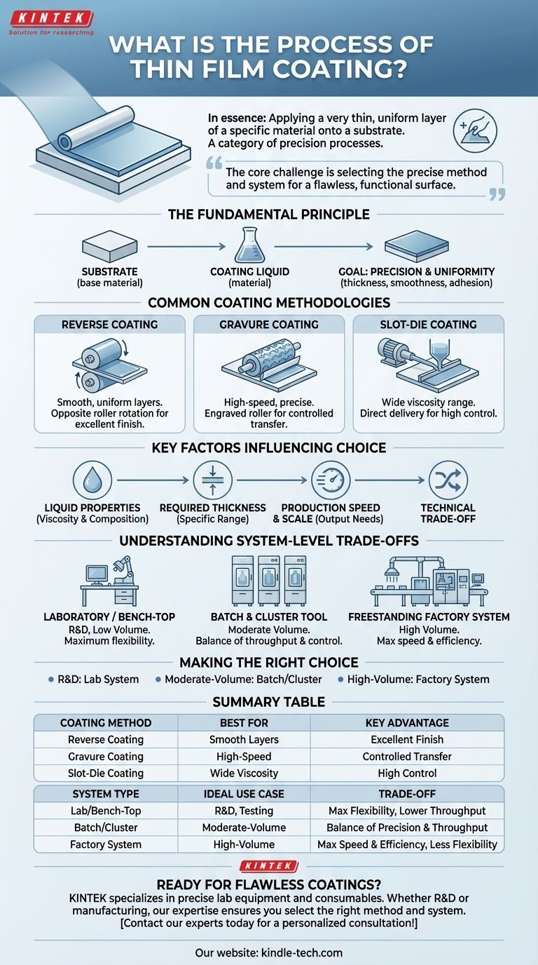
In essence, the process of thin film coating is the application of a very thin, uniform layer of a specific material onto a base surface, known as a substrate. This is not a single technique but a category of precision processes, with common methods including reverse coating, gravure coating, and slot-die coating, each chosen based on the specific application's needs.
The core challenge in thin film coating isn't just applying a layer; it's selecting the precise method and system that matches the coating material, the desired film thickness, and the required production scale to achieve a flawless, functional surface.
The Fundamental Principle of Coating
A Substrate and a Coating Material
At its heart, every thin film process involves two key components: the substrate (the base material being coated) and the coating liquid or material. The goal is to deposit the coating material onto the substrate with exceptional uniformity and controlled thickness.
The Goal: Precision and Uniformity
The process is considered successful when the final film meets strict specifications for thickness, smoothness, and adhesion. These properties are critical for the final product's performance, whether it's an electronic display, a medical device, or advanced packaging.
Common Coating Methodologies
The method chosen is determined by factors like the viscosity of the coating liquid, the target thickness, and the required production speed.
Reverse Coating
This method uses two rollers rotating in opposite directions at the point of application. The substrate passes through one roller while the coating is applied by the other, creating a very smooth and uniform layer.
Gravure Coating
Gravure coating uses a roller that is engraved with a pattern of very small cells. This roller picks up the coating liquid, and a doctor blade removes the excess, leaving a precise amount in the cells to be transferred to the substrate.
Slot-Die Coating
In this process, the coating liquid is precisely pumped through a narrow internal slot and delivered directly onto the moving substrate. This method offers excellent control over the thickness and width of the coating.
Key Factors Influencing Your Choice
The decision to use one method over another is a technical trade-off driven by the project's specific requirements.
The Coating Liquid's Properties
The viscosity (thickness) and chemical composition of the coating material are paramount. Some methods, like slot-die, handle a wide range of viscosities well, while others are more specialized.
Required Film Thickness
Different methods excel at producing different thickness ranges. A process ideal for an ultra-thin optical layer might be unsuitable for a thicker adhesive coating.
Production Speed and Scale
The required output dictates the choice. High-speed, roll-to-roll manufacturing often relies on methods like gravure or slot-die, while other applications may prioritize precision over speed.
Understanding the System-Level Trade-offs
The coating method is only part of the equation; the machinery or "system" that implements it is equally important. This choice reflects a trade-off between scale, flexibility, and cost.
Laboratory or Bench-Top Systems
These are small-scale systems designed for research, development, and low-volume experimental applications. They offer maximum flexibility to test different materials and processes.
Batch and Cluster Tool Systems
Batch systems process multiple substrates (like silicon wafers) at once in a single chamber. Cluster tools use multiple, interconnected chambers, allowing for a sequence of different processes without breaking the vacuum, offering a balance between throughput and control.
Freestanding Factory Systems
These are large, highly automated systems designed for high-volume, continuous production. They are optimized for a specific process to maximize speed, efficiency, and consistency in a manufacturing environment.
Making the Right Choice for Your Goal
- If your primary focus is research and material testing: A flexible laboratory or bench-top system is the ideal choice to experiment with different methods and formulations.
- If your primary focus is controlled, moderate-volume production: Batch or cluster tool systems provide the necessary precision and throughput for specialized manufacturing.
- If your primary focus is high-volume, cost-sensitive manufacturing: A dedicated, large-scale factory system using a high-speed method like gravure or slot-die is required.
Ultimately, mastering the process of thin film coating means aligning the right technique with the right production system to meet your specific performance and business goals.
Summary Table:
| Coating Method | Best For | Key Advantage |
|---|---|---|
| Reverse Coating | Smooth, uniform layers | Opposite roller rotation for excellent finish |
| Gravure Coating | High-speed, precise application | Engraved roller for controlled material transfer |
| Slot-Die Coating | Wide viscosity range, precise thickness | Direct delivery from a slot for high control |
| System Type | Ideal Use Case | Trade-off |
| Lab/Bench-Top | R&D, material testing | Maximum flexibility, lower throughput |
| Batch/Cluster Tool | Moderate-volume production | Balance of precision and throughput |
| Factory System | High-volume manufacturing | Maximum speed and efficiency, less flexibility |
Ready to achieve flawless thin film coatings for your laboratory or production line?
KINTEK specializes in providing the precise lab equipment and consumables you need to master the thin film coating process. Whether you are in R&D or full-scale manufacturing, our expertise ensures you select the right coating method and system—from flexible bench-top units to high-volume production tools—to meet your exact specifications for thickness, uniformity, and adhesion.
Let us help you optimize your coating process for superior results. Contact our experts today for a personalized consultation!
Visual Guide
Related Products
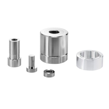
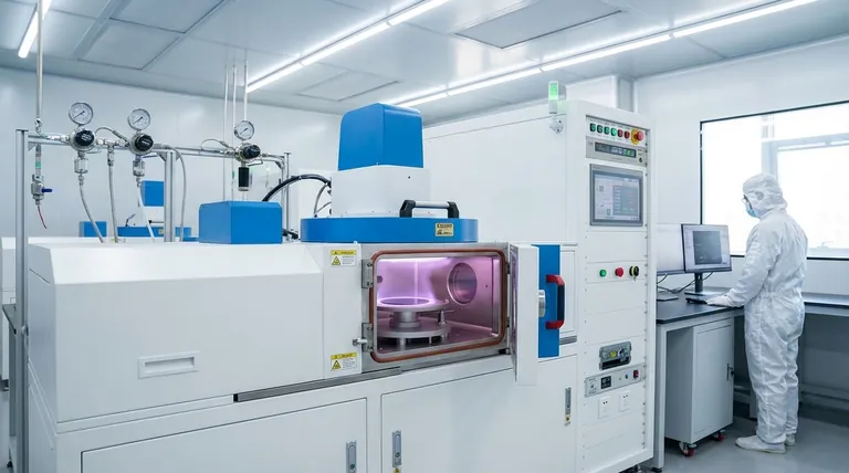
- HFCVD Machine System Equipment for Drawing Die Nano-Diamond Coating
- Ring Press Mold for Lab Applications
People Also Ask
- What is the chemical vapor deposition growth process? Build Superior Thin Films from the Atom Up
- What is the specific function of the metal filament in HF-CVD? Key Roles in Diamond Growth
- What is the function of tungsten filaments in HFCVD? Powering Diamond Film Synthesis with Thermal Excitation
- What types of substrates are used in CVD to facilitate graphene films? Optimize Graphene Growth with the Right Catalyst
- What are the advantages of chemical vapor deposition? Achieve Superior Thin Films for Your Lab