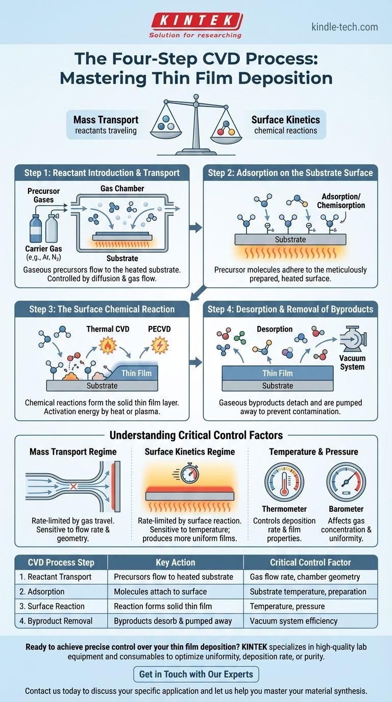
At its core, Chemical Vapor Deposition (CVD) is a multi-step process where gaseous chemical precursors react on a heated substrate surface to form a high-quality solid film. The fundamental sequence involves introducing reactant gases into a chamber, transporting them to the substrate, allowing them to react on the surface to build the film, and finally, removing the gaseous byproducts of that reaction.
The key to mastering CVD is recognizing it not as a single "coating" event, but as a delicate balance between two competing phenomena: the rate at which reactant gases can travel to the substrate (mass transport) and the rate at which they can chemically react on its surface (surface kinetics).
The Foundational Stages of CVD
To truly understand the process, we must break it down into its distinct physical and chemical stages. Each step is a critical control point that determines the final properties of the deposited film.
Step 1: Reactant Introduction and Transport
The process begins by introducing a controlled mixture of precursor gases into the reaction chamber. These are the chemical building blocks of your final film.
These precursors are often mixed with a diluent or carrier gas, typically an inert gas like argon or nitrogen. This mixture doesn't just passively fill the chamber; it flows toward the substrate. The movement of gas species to the substrate surface is a critical mass transport step governed by diffusion and gas flow dynamics.
Step 2: Adsorption on the Substrate Surface
For a reaction to occur, the precursor molecules must first physically attach to the substrate. This process is called adsorption.
The substrate surface must be meticulously prepared—cleaned and heated to a specific temperature—to ensure the precursor molecules can adhere uniformly. This initial attachment, or chemisorption, creates the necessary conditions for the chemical reaction to proceed.
Step 3: The Surface Chemical Reaction
This is the heart of the CVD process. Once adsorbed on the hot substrate, the precursor molecules gain enough energy to break their chemical bonds and react. This surface reaction forms the desired solid material, which deposits and builds up layer by layer, creating the thin film.
The energy needed to drive this reaction, known as activation energy, is typically supplied by heat (Thermal CVD) or by creating a plasma in the chamber (Plasma-Enhanced CVD or PECVD).
Step 4: Desorption and Removal of Byproducts
The chemical reactions that form the film also create unwanted gaseous byproducts. These byproducts must detach from the substrate surface (desorption) and be efficiently removed from the reaction chamber.
A vacuum system continuously pumps these byproducts out. If they are not removed, they can contaminate the film or interfere with the ongoing deposition reaction, negatively impacting film quality.
Understanding the Critical Control Factors
The success of a CVD process hinges on precisely controlling the variables that influence each of the stages described above. The final film quality is a direct result of how these factors are managed.
The Mass Transport Regime
In some conditions, the rate-limiting step is simply how fast reactant molecules can get to the surface. This is known as the mass-transport-limited regime. In this state, deposition is highly sensitive to gas flow rates and the geometry of the chamber.
The Surface Kinetics Regime
Alternatively, the process can be limited by how fast the chemical reaction can occur on the surface. This is the surface-reaction-limited regime (or kinetic-limited). Here, deposition is highly sensitive to temperature, as heat provides the energy for the reaction. This regime often produces more uniform films.
The Importance of Temperature and Pressure
Temperature is arguably the most critical parameter in CVD. It directly controls the deposition rate and influences the film's crystal structure, density, and stress.
Pressure within the chamber affects the concentration of reactant gases and how they travel. Lower pressures increase the "mean free path" of gas molecules, which can improve film uniformity.
Substrate Preparation is Non-Negotiable
A pristine, chemically active surface is essential for the film to adhere properly and grow uniformly. Steps like thermal dehydration to remove moisture or pre-deposition etching are often required to prepare the substrate for optimal growth.
Making the Right Choice for Your Goal
Understanding these steps allows you to troubleshoot the process and tailor it to achieve specific material properties.
- If your primary focus is high uniformity across a large area: You should aim to operate in the surface-reaction-limited regime by carefully controlling temperature and ensuring it is consistent across the entire substrate.
- If your primary focus is a high deposition rate: You can increase the reactant concentration and temperature, but be aware this may push you into the mass-transport-limited regime, potentially sacrificing uniformity.
- If your primary focus is film purity: You must use high-purity precursor gases and ensure your system has an efficient vacuum pump to rapidly remove reaction byproducts.
By mastering the interplay of gas transport and surface chemistry, you gain precise control over the synthesis of advanced materials.
Summary Table:
| CVD Process Step | Key Action | Critical Control Factor |
|---|---|---|
| 1. Reactant Transport | Gaseous precursors flow to the heated substrate | Gas flow rate, chamber geometry |
| 2. Adsorption | Precursor molecules attach to the substrate surface | Substrate temperature, surface preparation |
| 3. Surface Reaction | Chemical reaction forms the solid thin film | Temperature (thermal/PECVD), pressure |
| 4. Byproduct Removal | Gaseous byproducts desorb and are pumped away | Vacuum system efficiency |
Ready to achieve precise control over your thin film deposition? The quality of your CVD process directly impacts your research and production outcomes. KINTEK specializes in high-quality lab equipment and consumables for all your laboratory needs. Our experts can help you select the ideal CVD system or components to optimize your process for uniformity, deposition rate, or purity. Contact us today to discuss your specific application and let us help you master your material synthesis.
Visual Guide
Related Products
- CVD Diamond Dressing Tools for Precision Applications
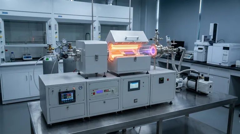
- Multi Heating Zones CVD Tube Furnace Machine Chemical Vapor Deposition Chamber System Equipment
- CVD Diamond Domes for Industrial and Scientific Applications
- CVD Diamond for Thermal Management Applications
- Chemical Vapor Deposition CVD Equipment System Chamber Slide PECVD Tube Furnace with Liquid Gasifier PECVD Machine
People Also Ask
- How do CVD diamonds grow? A Step-by-Step Guide to Lab-Grown Diamond Creation
- Can CVD diamonds change color? No, their color is permanent and stable.
- How do you identify a CVD diamond? The Definitive Guide to Lab-Grown Diamond Verification
- What is CVD diamond? The Ultimate Guide to Lab-Grown Diamonds and Their Uses
- How long does it take to make synthetic diamonds? Discover the 6-8 Week Science Behind Lab-Grown Gems


