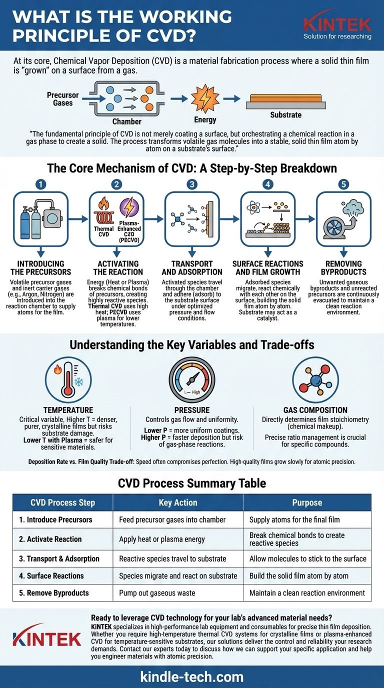
At its core, Chemical Vapor Deposition (CVD) is a material fabrication process where a solid thin film is "grown" on a surface from a gas. This is accomplished by introducing precursor gases into a reaction chamber, which then undergo a controlled chemical reaction upon activation by energy—typically heat or plasma. The result of this reaction is the formation of a new, solid material that deposits onto a target object, known as a substrate.
The fundamental principle of CVD is not merely coating a surface, but orchestrating a chemical reaction in a gas phase to create a solid. The process transforms volatile gas molecules into a stable, solid thin film atom by atom on a substrate's surface.
The Core Mechanism of CVD: A Step-by-Step Breakdown
To truly understand CVD, it's best to view it as a sequence of carefully controlled physical and chemical events. Each step is critical for the formation of a high-quality film.
Step 1: Introducing the Precursors
The process begins by feeding one or more volatile precursor gases into a reaction chamber. These gases contain the atoms required for the final film (e.g., methane gas, CH₄, as a source of carbon for diamond films).
Often, these precursors are diluted with an inert carrier gas, such as argon or nitrogen. This carrier gas helps to stabilize the process and precisely control the transport of the reactive molecules to the substrate.
Step 2: Activating the Reaction
The precursor gases are generally stable at room temperature and need an injection of energy to break their chemical bonds and become reactive. This is the most defining step of any CVD process.
There are two primary methods of activation:
- Thermal CVD: The substrate is heated to a high temperature, often several hundred degrees Celsius (e.g., 800-900°C for diamond). When the precursor gases contact the hot surface, they gain enough thermal energy to decompose and react.
- Plasma-Enhanced CVD (PECVD): An electric field (such as RF or microwave energy) is used to ionize the gases into a plasma. This plasma contains highly reactive ions and radicals, which can form a film at much lower temperatures, making it suitable for heat-sensitive substrates.
Step 3: Transport and Adsorption
Once activated, these reactive atomic and molecular species travel through the chamber and land on the substrate's surface. This process of sticking to the surface is called adsorption.
The conditions inside the chamber, such as pressure and gas flow, are optimized to ensure these species arrive at the substrate uniformly.
Step 4: Surface Reactions and Film Growth
This is where the film is built. The adsorbed species migrate across the substrate surface, find energetically favorable sites, and undergo chemical reactions with each other. These reactions create the desired solid material.
The film grows in a highly controlled, often layer-by-layer or atom-by-atom fashion. The substrate itself can act as a catalyst, providing a template that ensures the deposited film adheres strongly and grows with a specific crystalline structure.
Step 5: Removing Byproducts
The chemical reactions that form the film also create unwanted gaseous byproducts. These, along with any unreacted precursor gases, are continuously pumped out of the chamber to maintain a clean and controlled reaction environment.
Understanding the Key Variables and Trade-offs
The quality, properties, and even the type of material deposited via CVD are dictated by a delicate balance of process parameters. Understanding these trade-offs is key to mastering the technique.
Temperature: The Reaction's Conductor
Substrate temperature is arguably the most critical variable. Higher temperatures generally provide more energy for surface reactions, leading to denser, purer, and more crystalline films. However, high temperatures can damage sensitive substrates like plastics or pre-existing electronic components.
Pressure: Controlling Uniformity and Reaction Location
The chamber pressure influences how gas molecules travel. Lower pressures mean molecules travel in straighter lines, leading to more uniform coatings (better "line-of-sight" deposition). Higher pressures can increase the deposition rate but risk causing reactions in the gas phase before reaching the substrate, which can result in powder formation instead of a quality film.
Gas Composition: The Material's Blueprint
The ratio of precursor and carrier gases directly determines the chemical makeup (stoichiometry) of the final film. For example, in depositing silicon nitride (Si₃N₄), the ratio of silicon-containing gas to nitrogen-containing gas must be precisely managed to achieve the correct material properties.
Deposition Rate vs. Film Quality
There is an inherent trade-off between speed and perfection. Attempting to deposit a film too quickly by increasing gas flow or temperature can introduce defects, impurities, and internal stresses. High-quality films, like those for semiconductors or lab-grown diamonds, are often grown very slowly over hours or even days to ensure atomic precision.
How to Apply This to Your Project
Your choice of CVD parameters should be driven by the specific requirements of your final product.
- If your primary focus is high-purity, crystalline films (e.g., for semiconductors, optical coatings): You will likely require a high-temperature Thermal CVD process to achieve the necessary film quality and structural integrity.
- If your primary focus is coating temperature-sensitive materials (e.g., polymers, flexible electronics): Plasma-Enhanced CVD (PECVD) is the essential choice, as it enables deposition at significantly lower temperatures.
- If your primary focus is depositing a specific chemical compound (e.g., titanium nitride, silicon carbide): Your main challenge is the precise control over the flow rates and partial pressures of multiple precursor gases to ensure correct stoichiometry.
By understanding these core principles, you can effectively leverage CVD to engineer materials with precision from the atom up.
Summary Table:
| CVD Process Step | Key Action | Purpose |
|---|---|---|
| 1. Introduce Precursors | Feed precursor gases into chamber | Supply atoms for the final film |
| 2. Activate Reaction | Apply heat or plasma energy | Break chemical bonds to create reactive species |
| 3. Transport & Adsorption | Reactive species travel to substrate | Allow molecules to stick to the surface |
| 4. Surface Reactions | Species migrate and react on substrate | Build the solid film atom by atom |
| 5. Remove Byproducts | Pump out gaseous waste | Maintain a clean reaction environment |
Ready to leverage CVD technology for your lab's advanced material needs? KINTEK specializes in high-performance lab equipment and consumables for precise thin film deposition. Whether you require high-temperature thermal CVD systems for crystalline films or plasma-enhanced CVD for temperature-sensitive substrates, our solutions deliver the control and reliability your research demands. Contact our experts today to discuss how we can support your specific application and help you engineer materials with atomic precision.
Visual Guide
Related Products
- CVD Diamond Dressing Tools for Precision Applications
- Multi Heating Zones CVD Tube Furnace Machine Chemical Vapor Deposition Chamber System Equipment
- CVD Diamond Domes for Industrial and Scientific Applications
- CVD Diamond for Thermal Management Applications
- Chemical Vapor Deposition CVD Equipment System Chamber Slide PECVD Tube Furnace with Liquid Gasifier PECVD Machine
People Also Ask
- How do you identify a CVD diamond? The Definitive Guide to Lab-Grown Diamond Verification
- Can CVD diamonds change color? No, their color is permanent and stable.
- What are the disadvantages of CVD diamonds? Understanding the trade-offs for your purchase.
- Does the chemical vapor deposition be used for diamonds? Yes, for Growing High-Purity Lab Diamonds
- What color diamonds are CVD? Understanding the Process from Brown Tint to Colorless Beauty


