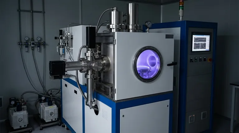
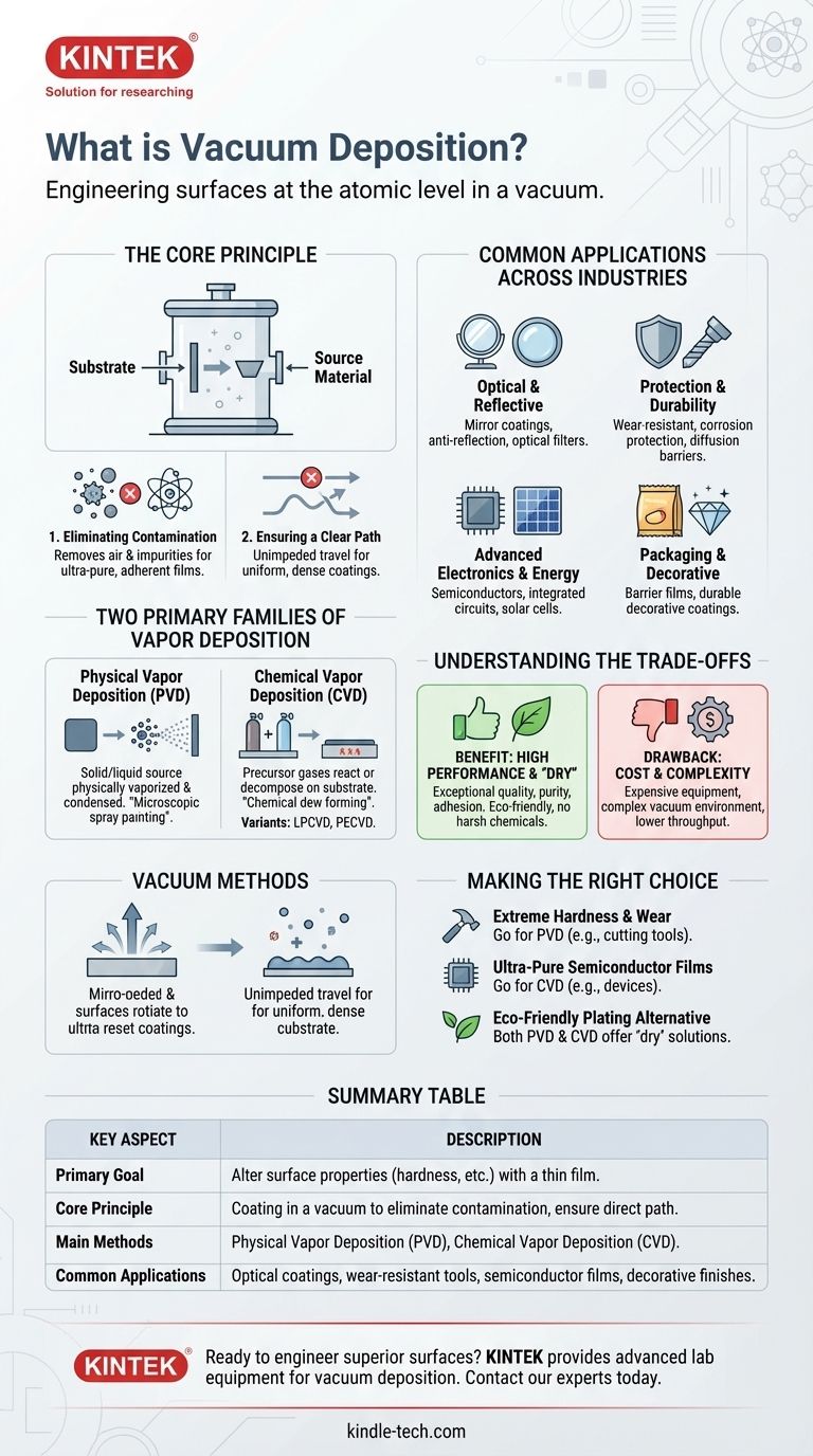
In essence, vacuum deposition is a family of processes used to apply an exceptionally thin, high-performance coating of material onto a surface, known as a substrate. This entire process takes place inside a vacuum chamber, which is critical for creating pure, dense, and highly adherent films for an enormous range of industrial and technical applications.
The core purpose of vacuum deposition is not simply to coat an object, but to fundamentally alter its surface properties. By creating a film at the atomic or molecular level, this technique can make a material harder, more reflective, electrically conductive, or resistant to corrosion.
Why Use a Vacuum? The Core Principle
Eliminating Contamination
The primary reason for using a vacuum is to remove air and other gaseous particles from the chamber.
These particles would otherwise interfere with the process, reacting with the coating material and creating impurities in the final film. The vacuum ensures the coating is exceptionally pure.
Ensuring a Clear Path
In a vacuum, the vaporized coating material can travel from its source to the substrate in a straight line, unimpeded by collisions with air molecules.
This direct path is essential for creating a uniform and dense coating. Without it, the process would be uncontrolled and the resulting film would be of poor quality.
The Two Primary Families of Vapor Deposition
Vapor deposition methods are broadly divided into two major categories based on how the coating material is generated and transported to the substrate.
Physical Vapor Deposition (PVD)
In PVD, a solid or liquid source material is physically converted into a vapor and transported to the substrate, where it condenses back into a solid film.
Think of it as a microscopic form of spray painting, where individual atoms or molecules are the "paint." The material is simply moved from a source to the target without undergoing a fundamental chemical change.
Chemical Vapor Deposition (CVD)
In CVD, the substrate is exposed to one or more volatile precursor gases which then react or decompose on the substrate's surface to produce the desired solid coating.
This is more like dew forming on a cold surface, but instead of water condensing, a chemical reaction on the surface builds the film layer by layer. There are many variations, such as Low-Pressure CVD (LPCVD) and Plasma-Enhanced CVD (PECVD), tailored for specific materials and applications.
Common Applications Across Industries
Vacuum deposition is a foundational technology in modern manufacturing, used to create products we rely on every day.
Optical and Reflective Properties
These coatings are used to control the reflection and transmission of light. Applications include mirror coatings, anti-reflection coatings on eyeglasses and camera lenses, and optical interference filters.
Protection and Durability
By applying a very hard layer of material, vacuum deposition can dramatically increase the lifespan of tools and components. This includes wear-resistant coatings on machine tools, corrosion-protective coatings, and diffusion barriers.
Advanced Electronics and Energy
The precision of vacuum deposition is critical for manufacturing modern electronics. It's used to create the electrically conducting films in semiconductor devices, integrated circuits, and solar cells.
Packaging and Decorative Finishes
The technology is used to apply permeation barrier films on flexible packaging to keep food fresh. It is also used for creating durable and attractive decorative coatings on everything from automotive parts to home fixtures.
Understanding the Trade-offs
While powerful, vacuum deposition is a specialized process with distinct advantages and disadvantages.
The Benefit: High Performance and a 'Dry' Process
The primary advantage is the exceptional quality, purity, and adhesion of the resulting films.
Furthermore, because these are 'dry' processes that do not use harsh liquid chemicals, they are often considered more environmentally friendly than traditional wet processes like electroplating with chromium or cadmium.
The Drawback: Cost and Complexity
Vacuum deposition equipment is expensive to purchase and operate. The processes require a controlled vacuum environment, which adds complexity and can result in lower throughput compared to other coating methods.
Making the Right Choice for Your Goal
Selecting the correct approach depends entirely on the desired properties of the final product.
- If your primary focus is extreme hardness for cutting tools or wear parts: Physical Vapor Deposition (PVD) is a common and effective choice.
- If your primary focus is creating ultra-pure, uniform films for semiconductor devices: Chemical Vapor Deposition (CVD) and its specialized variants are the industry standard.
- If your primary focus is replacing a hazardous plating process with an eco-friendly alternative: Both PVD and CVD offer high-performance, 'dry' process solutions.
Ultimately, vacuum deposition is a powerful toolkit for engineering surfaces with properties far beyond those of the underlying material.
Summary Table:
| Key Aspect | Description |
|---|---|
| Primary Goal | Alter surface properties (hardness, conductivity, reflectivity) with a thin film. |
| Core Principle | Coating takes place in a vacuum to eliminate contamination and ensure a direct particle path. |
| Main Methods | Physical Vapor Deposition (PVD) and Chemical Vapor Deposition (CVD). |
| Common Applications | Optical coatings, wear-resistant tools, semiconductor films, and decorative finishes. |
Ready to engineer superior surfaces? KINTEK specializes in providing advanced lab equipment and consumables for vacuum deposition processes. Whether you're developing new coatings for optics, electronics, or durable components, our solutions support the precision and purity your R&D or production demands. Contact our experts today to discuss how we can enhance your laboratory's capabilities.
Visual Guide
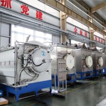
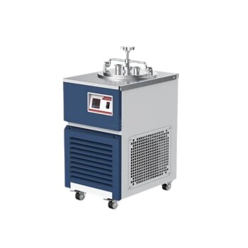
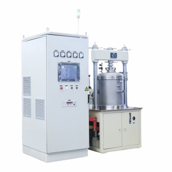
Related Products
- Split Chamber CVD Tube Furnace with Vacuum Station Chemical Vapor Deposition System Equipment Machine
- Chemical Vapor Deposition CVD Equipment System Chamber Slide PECVD Tube Furnace with Liquid Gasifier PECVD Machine
- HFCVD Machine System Equipment for Drawing Die Nano-Diamond Coating
- Customer Made Versatile CVD Tube Furnace Chemical Vapor Deposition Chamber System Equipment
- Inclined Rotary Plasma Enhanced Chemical Vapor Deposition PECVD Equipment Tube Furnace Machine
People Also Ask
- What is a CVD tube furnace? A Complete Guide to Thin-Film Deposition
- What is the function of a tube furnace in CVD SiC synthesis? Achieving Ultra-Pure Silicon Carbide Powders
- What is the function of a high-temperature CVD tube furnace in 3D graphene foam prep? Master 3D Nanomaterial Growth
- What is a split tube furnace? Unlock Unmatched Access for Complex Lab Setups
- What functions does a tube CVD furnace perform during the stabilization and carbonization of composite fibers?