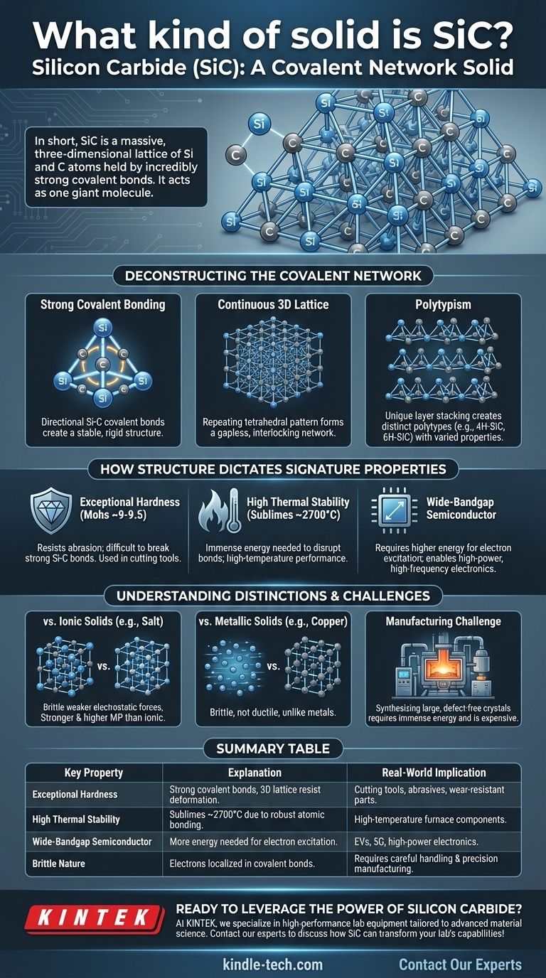
In short, Silicon Carbide (SiC) is a covalent network solid. This classification means its silicon and carbon atoms are locked into a massive, three-dimensional lattice held together by extremely strong and directional covalent bonds. Unlike molecular solids with weak forces between molecules, the entire crystal of SiC effectively acts as one single, giant molecule.
The classification of SiC as a covalent network solid is not just a label; it is the fundamental explanation for its exceptional properties. Understanding its rigid atomic lattice is the key to grasping its extreme hardness, high-temperature stability, and unique electronic behavior.
Deconstructing the Covalent Network Structure
To understand SiC, you must first visualize its underlying atomic architecture. It is this structure that dictates nearly all of its useful characteristics.
The Nature of Covalent Bonding in SiC
Silicon Carbide is formed from silicon (Si) and carbon (C) atoms. These two elements have a relatively small difference in electronegativity, causing them to share electrons and form very strong, stable covalent bonds.
These bonds are highly directional. Each carbon atom is bonded to four silicon atoms, and each silicon atom is bonded to four carbon atoms in a rigid tetrahedral arrangement.
A Continuous 3D Lattice
This tetrahedral bonding pattern repeats endlessly in all three dimensions. This creates a continuous, interlocking network with no weak points or individual molecules.
Think of it as a structure similar to diamond, but with alternating silicon and carbon atoms instead of just carbon. This rigid, gapless structure is the source of SiC's immense physical strength.
The Concept of Polytypism
A unique feature of SiC is polytypism. While the local Si-C tetrahedral bonding is constant, the layers of these tetrahedrons can be stacked in different sequences.
These different stacking arrangements create distinct crystal structures called polytypes, such as 4H-SiC and 6H-SiC. While all are SiC, these polytypes have slightly different electronic properties, making them suitable for different semiconductor applications.
How Structure Dictates SiC's Signature Properties
The covalent network model directly explains why SiC behaves the way it does. The material's macroscopic properties are a direct consequence of its microscopic bonding and structure.
Exceptional Hardness and Strength
To scratch or deform SiC, you must physically break the powerful Si-C covalent bonds. Because the entire crystal is a single network of these bonds, it exhibits incredible resistance to abrasion and deformation.
On the Mohs scale of hardness, SiC (~9-9.5) is second only to diamond (10), making it an elite material for cutting tools, abrasives, and wear-resistant components.
High Thermal Stability
Melting or breaking down a solid requires giving its atoms enough energy to overcome the forces holding them together. The immense strength of the Si-C covalent bonds means a vast amount of thermal energy is needed to disrupt the lattice.
Consequently, SiC does not melt at atmospheric pressure but instead sublimes (turns directly into a gas) at extremely high temperatures, around 2700 °C (4900 °F).
Unique Semiconductor Behavior
While the strong bonds are characteristic of an electrical insulator like diamond, the energy required to excite an electron into a conducting state (the bandgap) in SiC is less than in diamond.
This places SiC in a special category of wide-bandgap semiconductors. Its bandgap is significantly wider than that of pure silicon, allowing SiC-based electronics to operate at much higher voltages, temperatures, and frequencies.
Understanding the Trade-offs and Distinctions
Placing SiC in context with other solids clarifies its unique position. Its properties are a trade-off defined by its bonding.
SiC vs. Ionic Solids (e.g., Salt)
Ionic solids like sodium chloride (NaCl) are held together by non-directional electrostatic attraction between positive and negative ions. While they form crystals, these bonds are generally weaker than SiC's covalent bonds, making them softer and giving them much lower melting points.
SiC vs. Metallic Solids (e.g., Copper)
Metals are characterized by a "sea" of delocalized electrons surrounding a lattice of positive ions. This electron sea allows metals to be conductive and ductile (malleable). In contrast, SiC's electrons are locked in localized covalent bonds, making it a semiconductor and inherently brittle.
The Challenge of Manufacturing
The very strength that makes SiC so desirable also makes it incredibly difficult to produce. Synthesizing large, defect-free single crystals of SiC requires immense energy and sophisticated processes (like the Lely method), making it significantly more expensive than silicon.
Making the Right Choice for Your Application
Understanding SiC's classification as a covalent network solid allows you to predict its behavior and best use cases.
- If your primary focus is on mechanical performance: Recognize that its covalent network is the direct source of its top-tier hardness and wear resistance, making it ideal for abrasives, sandblasting, and durable mechanical seals.
- If your primary focus is on high-power electronics: Understand that its covalent network creates a wide-bandgap semiconductor, essential for building robust power inverters, EV chargers, and 5G communication modules that outperform silicon.
- If your primary focus is on material science: Classify SiC as a prototypical covalent network solid, using it as a benchmark for hardness and thermal stability when comparing against other advanced ceramics like boron nitride or silicon nitride.
Ultimately, knowing that Silicon Carbide is a covalent network solid is the first principle in understanding and applying its extraordinary capabilities.
Summary Table:
| Key Property | Explanation | Real-World Implication |
|---|---|---|
| Exceptional Hardness | Strong covalent bonds in a 3D lattice resist deformation. | Ideal for cutting tools, abrasives, and wear-resistant parts. |
| High Thermal Stability | Sublimes at ~2700°C due to robust atomic bonding. | Suitable for high-temperature applications like furnace components. |
| Wide-Bandgap Semiconductor | Electrons require more energy to excite, enabling high-power operation. | Used in EVs, 5G tech, and power electronics for superior performance. |
| Brittle Nature | Electrons are localized in covalent bonds, limiting ductility. | Requires careful handling and precision manufacturing processes. |
Ready to leverage the power of Silicon Carbide in your lab? At KINTEK, we specialize in providing high-performance lab equipment and consumables tailored to advanced material science needs. Whether you're developing next-generation semiconductors or require durable components for high-temperature processes, our expertise ensures you get the right solutions for superior results. Contact our experts today to discuss how SiC can transform your laboratory's capabilities!
Visual Guide
Related Products
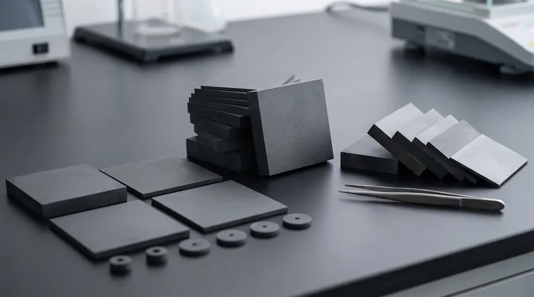
- Silicon Carbide (SIC) Ceramic Sheet Wear-Resistant Engineering Advanced Fine Ceramics
- Silicon Carbide (SIC) Ceramic Plate for Engineering Advanced Fine Ceramics
- Silicon Carbide (SIC) Ceramic Sheet Flat Corrugated Heat Sink for Engineering Advanced Fine Ceramics
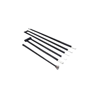
- Silicon Carbide SiC Thermal Heating Elements for Electric Furnace
- Precision Machined Silicon Nitride (SiN) Ceramic Sheet for Engineering Advanced Fine Ceramics
People Also Ask
- What is the type of silicon carbide? A Guide to Polymorphs, Grades, and Applications
- What are the properties and applications of silicon carbide ceramics? Solve Extreme Engineering Challenges
- What are the properties of SiC? Unlock High-Temperature, High-Frequency Performance
- Why is silicon carbide more efficient? Unlock Higher Power Density with SiC's Superior Material Properties
- What are the common uses of silicon carbide? Unlock Extreme Performance in Harsh Environments