At its core, Plasma-Enhanced Chemical Vapor Deposition (PECVD) is used to create a specific set of high-performance thin films. The most common materials deposited by this process are dielectric films like Silicon Nitride (SiNx) and Silicon Dioxide (SiO2), semiconductor films like amorphous Silicon (a-Si:H), and hard protective coatings like Diamond-Like Carbon (DLC) and graphene.
The crucial insight is not just what materials PECVD creates, but why it is chosen. PECVD uses plasma to deposit high-quality films at significantly lower temperatures than traditional CVD, making it essential for coating heat-sensitive materials like semiconductors and plastics.
Core Materials Deposited by PECVD
The versatility of PECVD stems from its ability to produce a range of functional thin films by carefully selecting precursor gases and process conditions. The materials created are typically categorized by their application.
Dielectric and Insulating Films
These films are fundamental to the electronics industry for isolating conductive layers.
- Silicon Nitride (SiNx): A robust material used as a passivation layer in microelectronics. It protects semiconductor devices from moisture and contamination.
- Silicon Dioxide (SiO2): An excellent electrical insulator. It is a building block for transistors, capacitors, and other components on integrated circuits.
Semiconductor Films
PECVD is critical for creating the active layers in certain electronic devices.
- Amorphous Hydrogenated Silicon (a-Si:H): This material is the foundation of many thin-film transistors (TFTs), which are used in LCD screens, and is also a key component in thin-film solar cells.
Carbon-Based Films
These films are prized for their unique mechanical and electrical properties.
- Diamond-Like Carbon (DLC): A class of extremely hard, low-friction coatings. DLC is applied to mechanical parts, cutting tools, and medical implants to dramatically improve wear resistance.
- Graphene: PECVD allows for the precisely controlled growth of graphene, including specialized structures like vertical graphene, for advanced electronics and research applications.
The Precursor Gases: The "Ingredients" of PECVD
The final thin film on the substrate is not placed there directly. Instead, it is formed from chemical reactions between precursor gases introduced into the vacuum chamber.
How Precursors Work
The process begins with one or more gases that contain the atoms needed for the final film (e.g., silicon, nitrogen, carbon). A powerful radio frequency (RF) signal energizes these gases into a plasma, breaking them apart into highly reactive species that then deposit onto the substrate surface to form the desired material.
Common Precursor Examples
The choice of gas determines the final film. For example, to create silicon nitride (SiNx), gases like silane (SiH4) and ammonia (NH3) are often used. The plasma breaks them down, allowing silicon and nitrogen atoms to combine on the substrate.
Understanding the Trade-offs
While powerful, PECVD is not a universal solution. Understanding its advantages and limitations is key to using it effectively.
Advantage: Lower Temperature Deposition
This is the primary reason for choosing PECVD. The plasma provides the energy for chemical reactions, eliminating the need for the extremely high temperatures required by traditional thermal CVD. This allows for coating on sensitive substrates like plastics, glass, and fully fabricated microchips without damaging them.
Limitation: Film Purity and Composition
Because the process uses precursor gases that often contain hydrogen (like silane), some of this hydrogen can be incorporated into the final film. This is sometimes intentional (as in a-Si:H) but can also be an impurity that affects the film's properties.
Limitation: Film Density and Stress
PECVD films can sometimes have lower density or different internal stress compared to films grown at higher temperatures. For applications where maximum density or specific stress characteristics are paramount, other methods might be more suitable.
Making the Right Choice for Your Application
Selecting the right deposition technology depends entirely on your material needs and substrate constraints.
- If your primary focus is semiconductor fabrication: PECVD is the industry standard for depositing high-quality SiNx and SiO2 insulating layers on devices that cannot withstand high process heat.
- If your primary focus is wear-resistant coatings: PECVD is a leading method for producing hard, low-friction DLC films for mechanical and decorative applications.
- If your primary focus is advanced research or photovoltaics: PECVD offers the control needed to create specialized films like amorphous silicon for solar cells and novel materials like graphene.
Ultimately, PECVD is the essential tool when you need to create high-performance inorganic films on substrates that require a low-temperature process.
Summary Table:
| Material Category | Key Materials | Primary Applications |
|---|---|---|
| Dielectric Films | Silicon Nitride (SiNx), Silicon Dioxide (SiO2) | Microelectronics, Passivation, Insulation |
| Semiconductor Films | Amorphous Hydrogenated Silicon (a-Si:H) | Thin-Film Transistors, Solar Cells |
| Carbon-Based Films | Diamond-Like Carbon (DLC), Graphene | Wear-Resistant Coatings, Advanced Electronics |
Need to deposit high-performance thin films on heat-sensitive materials? KINTEK specializes in PECVD lab equipment and consumables, providing the precise control and low-temperature capabilities essential for semiconductor fabrication, wear-resistant coatings, and advanced research. Let our experts help you select the right solution for your specific application. Contact us today to enhance your laboratory's thin-film deposition processes!
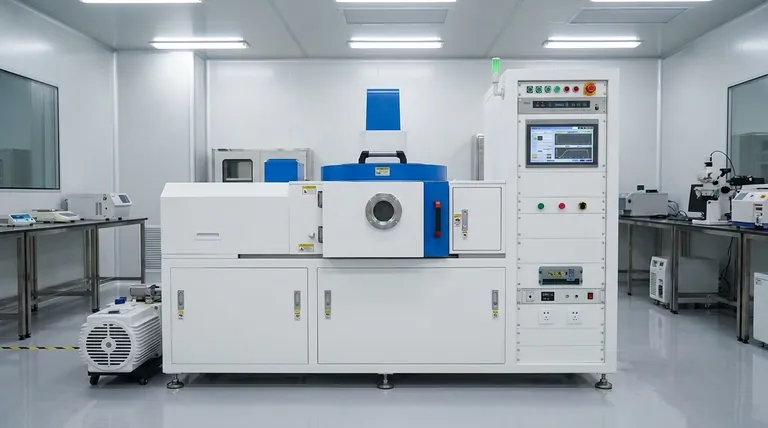
Visual Guide

Related Products
- Inclined Rotary Plasma Enhanced Chemical Vapor Deposition PECVD Equipment Tube Furnace Machine
- Chemical Vapor Deposition CVD Equipment System Chamber Slide PECVD Tube Furnace with Liquid Gasifier PECVD Machine
- Inclined Rotary Plasma Enhanced Chemical Vapor Deposition PECVD Equipment Tube Furnace Machine
- RF PECVD System Radio Frequency Plasma-Enhanced Chemical Vapor Deposition RF PECVD
- Multi Heating Zones CVD Tube Furnace Machine Chemical Vapor Deposition Chamber System Equipment
People Also Ask
- How does PECVD facilitate Ru-C nanocomposite films? Precision Low-Temperature Thin Film Synthesis
- What are the core advantages of PE-CVD in OLED encapsulation? Protect Sensitive Layers with Low-Temp Film Deposition
- Why is a PECVD system required for vertical graphene synthesis? Master Directional Control for 3D Nanostructures
- How does plasma enhanced chemical vapor deposition work? Enable Low-Temperature Thin Film Deposition
- What are the benefits of plasma enhanced CVD? Achieve High-Quality, Low-Temperature Film Deposition


