At their core, thin film semiconductor devices are built from a strategic stack of materials, primarily inorganic compounds, metals, and dielectrics. While the active semiconductor layer itself is often an inorganic compound like amorphous silicon or cadmium telluride, a functioning device requires conductive metals for contacts and insulating oxides or ceramics to direct the flow of electricity. The specific material for each layer is chosen based on its unique electronic, optical, and physical properties.
The selection of materials for a thin film semiconductor is not about finding a single perfect substance. It is about engineering a multi-layer system where each material—be it a semiconductor, a conductor, or an insulator—is chosen for its specific function and its ability to work in concert with the others.
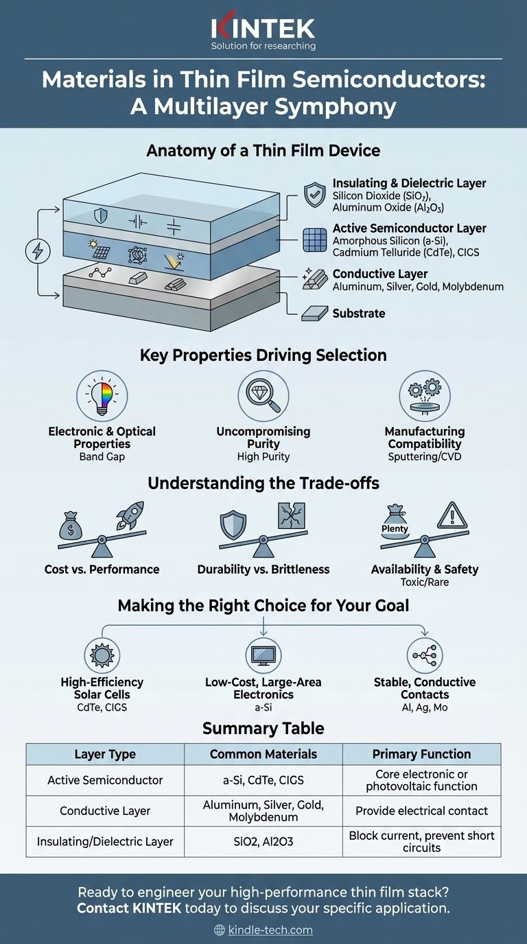
The Anatomy of a Thin Film Device
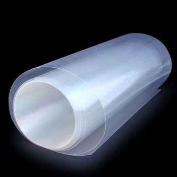
A "thin film semiconductor" is rarely a single layer. It is a precisely engineered stack of different materials, each deposited in a layer often no thicker than a few micrometers. Understanding these distinct layers is key to understanding the material choices.
The Active Semiconductor Layer
This is the heart of the device, responsible for the primary electronic or photovoltaic function. These materials must have specific electrical properties.
Common choices include inorganic compounds that can be deposited as a thin, uniform film. Examples are amorphous silicon (a-Si), cadmium telluride (CdTe), and copper indium gallium selenide (CIGS), which are widely used in solar cells.
Conductive Layers
To get electricity into and out of the active layer, you need conductive pathways. These are typically made from metals or conductive alloys.
Materials like aluminum, silver, gold, or molybdenum are chosen for their high conductivity and ability to form a good electrical contact with the semiconductor layer.
Insulating and Dielectric Layers
Controlling the flow of electricity is just as important as conducting it. Insulating layers prevent short circuits and are critical components in devices like transistors.
These layers are typically made from oxides and ceramics, such as silicon dioxide (SiO2) or aluminum oxide (Al2O3). They are chosen for their ability to block current (high electrical resistance) and withstand high electric fields.
Key Properties Driving Material Selection
The choice of a specific metal, oxide, or compound is not arbitrary. It is dictated by a strict set of requirements tied to performance, manufacturing, and reliability.
Electronic and Optical Properties
The primary driver is the material's electronic structure. For a semiconductor, its band gap determines which wavelengths of light it can absorb (for a solar cell) or how easily it can switch between an "on" and "off" state (for a transistor).
Uncompromising Purity
Thin film materials must be exceptionally pure. As noted in semiconductor supply chains, materials are often required at high purity and near theoretical densities.
Even minuscule amounts of impurities can introduce defects into the material's crystal structure. These defects act as traps for electrons, drastically degrading the device's electrical performance and reliability.
Manufacturing Compatibility
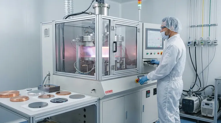
A material is only useful if it can be reliably deposited. Materials are chosen based on their suitability for processes like sputtering, evaporation, or chemical vapor deposition (CVD).
The material must be available in the correct form, such as a high-purity sputtering target or a precursor gas, to be used in these high-vacuum manufacturing techniques.
Understanding the Trade-offs
Every material choice involves a compromise. The ideal material rarely exists, so engineers must balance competing priorities to meet the application's goals.
Cost vs. Performance
There is a constant tension between device efficiency and cost. High-purity metals like gold offer excellent performance and stability but are expensive.
Conversely, more common materials may be cheaper but come with performance penalties, forcing a trade-off between the final product's price and its effectiveness.
Durability vs. Brittleness
Mechanical properties are also critical. While many oxides and ceramics are extremely durable and can withstand high temperatures, they are also often brittle.
This brittleness can be a significant drawback in applications requiring flexibility, such as wearable electronics, where a more pliable (but potentially less durable) material might be necessary.
Material Availability and Safety
Some of the best-performing semiconductor materials come with external challenges. For instance, cadmium used in CdTe solar cells is a toxic heavy metal, requiring strict environmental controls during manufacturing and disposal.
Similarly, materials like indium and gallium (used in CIGS and other compounds) are relatively rare, leading to concerns about price volatility and long-term supply chain stability.
Making the Right Choice for Your Goal
The optimal material stack depends entirely on the specific application you are designing for.
- If your primary focus is high-efficiency solar cells: You will likely use inorganic compounds like CdTe or CIGS, which have optimal bandgaps for absorbing the solar spectrum.
- If your primary focus is low-cost, large-area electronics: Amorphous silicon (a-Si) is a common choice due to its mature, scalable manufacturing process and acceptable performance for applications like display backplanes.
- If your primary focus is creating stable, conductive contacts: High-purity metals like aluminum, silver, or molybdenum are selected for their excellent conductivity and compatibility with standard deposition processes.
Ultimately, a successful thin film device is a precisely engineered symphony of materials, each chosen for its unique and essential role.
Summary Table:
| Layer Type | Common Materials | Primary Function |
|---|---|---|
| Active Semiconductor | Amorphous Silicon (a-Si), Cadmium Telluride (CdTe), CIGS | Core electronic or photovoltaic function (e.g., light absorption) |
| Conductive Layer | Aluminum, Silver, Gold, Molybdenum | Provide electrical contact and pathways for current |
| Insulating/Dielectric Layer | Silicon Dioxide (SiO₂), Aluminum Oxide (Al₂O₃) | Block current, prevent short circuits, control electricity flow |
Ready to engineer your high-performance thin film stack?
The right materials are critical for the efficiency, durability, and cost-effectiveness of your semiconductor devices. KINTEK specializes in providing the high-purity materials and expert support your laboratory needs.
We supply essential components like sputtering targets and high-purity metals and compounds, crucial for deposition processes like sputtering and evaporation.
Contact us today to discuss how our materials and expertise can help you build a better device. Let's talk about your specific application: Get in touch via our contact form.
Visual Guide
Related Products
- Customizable PTFE Wafer Carriers for Semiconductor and Lab Applications
- Electron Beam Evaporation Coating Oxygen-Free Copper Crucible and Evaporation Boat
- Custom PTFE Wafer Holders for Lab and Semiconductor Processing
- Conductive Carbon Cloth Carbon Paper Carbon Felt for Electrodes and Batteries
- Thin-Layer Spectral Electrolysis Electrochemical Cell
People Also Ask
- Why is slender PTFE tubing necessary for flow control in multi-channel catalyst aging? Ensure Equal Gas Distribution
- Why are PTFE containers required for PCT leaching tests? Ensure Chemical Inertness and Analytical Precision
- What are the specific applications of PTFE in micro-batch slug flow systems? Enhance Your Microfluidic Reaction Purity
- What is the function of a customized PTFE cap in IL-TEM? Bridge the Gap Between Microscopy and Electrochemistry
- Are semiconductors thin or thick? Discover the Power of Microscopic Thinness in Modern Electronics