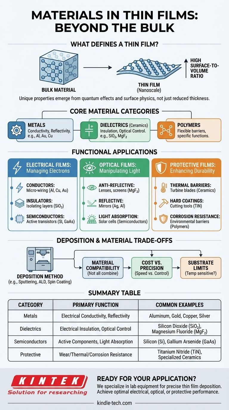
At its core, a thin film can be made from a wide range of materials, primarily categorized as metals, dielectrics (a class of ceramics), and polymers. The specific material is chosen not for its bulk properties, but for the unique electrical, optical, or mechanical characteristics it exhibits when reduced to a layer just a few atoms or micrometers thick.
The choice of a thin film material is never arbitrary. It is dictated entirely by the film's intended function—whether it needs to manage electrons (electrical films) or photons (optical films), or provide a protective barrier.
What Defines a Thin Film?
A common misconception is that a "thin film" is simply any material made into a thin layer. The reality is more fundamental.
More Than Just Thickness
A material becomes a true thin film when its thickness is so minimal that its surface-to-volume ratio drastically increases. This change causes quantum effects and surface physics to dominate over the material's normal bulk properties, unlocking new behaviors.
The Atomic-Scale Behavior
This transformation is driven by processes at the atomic level. Key behaviors like adsorption (atoms sticking to the surface), desorption (atoms leaving the surface), and surface diffusion (atoms moving across the surface) become the defining characteristics of the material, enabling its unique function.
The Functional Categories of Thin Film Materials
The vast array of materials used in thin films can be understood by grouping them by their primary application. This functional approach clarifies why a specific material is selected.
Electrical Films: Conductors, Insulators, and Semiconductors
These films form the bedrock of all modern electronics.
- Conductors: Metals like aluminum, copper, gold, and tungsten are used to create the microscopic wiring in integrated circuits.
- Insulators: Dielectric materials, such as silicon dioxide (SiO₂) or high-k ceramics, are used to isolate conductive layers and build capacitors.
- Semiconductors: Materials like silicon (Si) and gallium arsenide (GaAs) are the active components, forming the transistors that power our devices.
Optical Films: Manipulating Light
These films are designed to control the flow of light for applications ranging from solar cells to advanced displays.
- Anti-Reflective Coatings: Multiple layers of dielectric materials like magnesium fluoride (MgF₂) and silicon dioxide are used to minimize reflection on lenses and screens.
- Reflective Coatings: Highly reflective metals like silver and aluminum are deposited to create mirrors and other reflective surfaces.
- Light Absorption: In solar cells, specific semiconductor films are engineered to efficiently absorb photons and convert their energy into electricity.
Protective and Mechanical Films: Enhancing Durability
This category focuses on using thin films to protect a substrate from its environment.
- Thermal Barriers: Specialized ceramics are deposited onto components like turbine blades in aerospace to protect them from extreme heat.
- Hard Coatings: Extremely hard materials like titanium nitride (TiN) are used to coat cutting tools, increasing their lifespan and performance.
- Corrosion Resistance: Inert polymers or metals are used to create a barrier that prevents oxidation and chemical damage.
Understanding the Trade-offs: Deposition and Material Choice
The material itself is only one part of the equation. The method used to create the film—the deposition process—introduces critical trade-offs that impact the final result.
The Link Between Method and Material
Not all materials can be deposited with every technique. Polymers, for example, are often applied using a liquid-phase method like spin coating. In contrast, hard metals and ceramics typically require a physical vapor deposition (PVD) method like sputtering or a chemical vapor deposition (CVD) process.
Cost vs. Precision
Deposition methods vary enormously in cost and complexity. Simple thermal evaporation is relatively inexpensive but offers less control. Advanced techniques like Atomic Layer Deposition (ALD) provide single-atom layer precision but come at a significantly higher cost and slower speed.
Substrate and Environmental Compatibility
The chosen deposition process must be compatible with the object being coated (the substrate). High-temperature CVD, for instance, cannot be used on a temperature-sensitive plastic substrate. The energy and chemistry of the process dictate which material-substrate combinations are feasible.
Making the Right Choice for Your Application
Selecting the right material requires aligning its properties and associated deposition method with your primary technical goal.
- If your primary focus is electrical performance: You will choose from metals for conductivity, dielectrics for insulation, and specific semiconductors for active device functionality.
- If your primary focus is optical control: Your choice will center on stacks of dielectric materials for anti-reflection or specific metals for high reflectivity.
- If your primary focus is surface protection: You will look to hard ceramics for wear resistance or inert polymers and metals for environmental barriers.
Ultimately, mastering thin film technology comes from understanding the fundamental link between a material's properties, its function at the nanoscale, and the process used to create it.
Summary Table:
| Material Category | Primary Function | Common Examples |
|---|---|---|
| Metals | Electrical Conductivity, Reflectivity | Aluminum, Gold, Copper, Silver |
| Dielectrics (Ceramics) | Electrical Insulation, Optical Control | Silicon Dioxide (SiO₂), Magnesium Fluoride (MgF₂) |
| Semiconductors | Active Electronic Components, Light Absorption | Silicon (Si), Gallium Arsenide (GaAs) |
| Protective Coatings | Wear Resistance, Thermal Barriers, Corrosion Protection | Titanium Nitride (TiN), Specialized Ceramics, Polymers |
Ready to select the perfect thin film material for your lab's specific application? At KINTEK, we specialize in lab equipment and consumables for thin film deposition, helping you achieve precise electrical, optical, or protective performance. Whether you're working with metals, dielectrics, or polymers, our expertise ensures optimal results for your research or production needs. Contact our team today to discuss your project and discover how KINTEK can support your laboratory's thin film innovation.
Visual Guide
Related Products
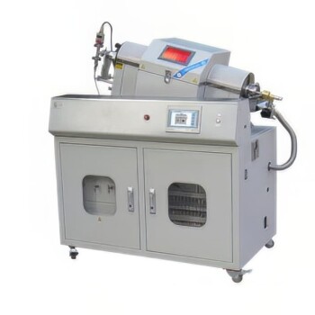
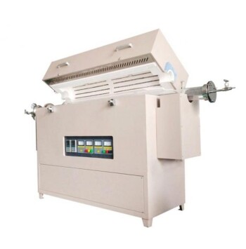
- Inclined Rotary Plasma Enhanced Chemical Vapor Deposition PECVD Equipment Tube Furnace Machine
- Vacuum Hot Press Furnace Machine for Lamination and Heating
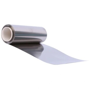
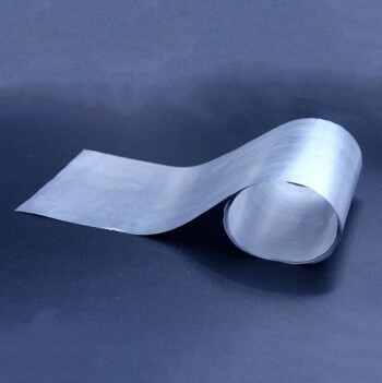
- High-Purity Titanium Foil and Sheet for Industrial Applications
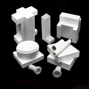
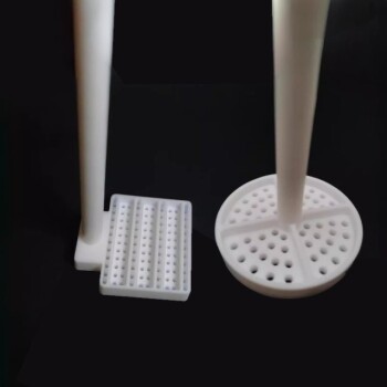
- Custom Machined and Molded PTFE Teflon Parts Manufacturer for Laboratory ITO FTO Conductive Glass Cleaning Flower Basket
- Lab Plastic PVC Calender Stretch Film Casting Machine for Film Testing
People Also Ask
- How does a sputtering machine work? Achieve Atomic-Level Precision for Your Coatings
- Is sputtering a PVD? Discover the Key Coating Technology for Your Lab
- What are the effects of magnetron sputtering? Achieve High-Quality, Durable Thin Films for Your Lab
- What is the RF frequency for sputtering? Unlocking the Standard for Insulating Materials
- What is a sputtering system? Achieve Unmatched Thin Film Deposition for Your Lab