Dual-plasma systems are utilized in advanced Silicon Carbide (SiC) CVD to decouple the generation of plasma species from the energy with which they strike the substrate. By combining Inductively Coupled Plasma (ICP) for density control and Radio Frequency (RF) bias for energy regulation, these systems solve the critical conflict between deposition efficiency and film damage.
The core advantage of this architecture is the independent control of chemical dissociation and physical ion bombardment, allowing for the rapid growth of high-quality films without the structural damage inherent in coupled plasma methods.
The Mechanics of Independent Control
Separation of Density and Energy
In traditional single-source plasma systems, increasing power to boost deposition rates invariably increases the impact energy of ions. This often damages the delicate crystal structure of the growing film.
Dual-plasma systems eliminate this coupling. They provide two separate "knobs" for the process engineer: one for creating the plasma cloud and one for directing it.
The Role of the ICP Source
The Inductively Coupled Plasma (ICP) source is responsible for the chemical side of the equation. Its primary function is to generate high concentrations of reactive radicals.
By controlling the ICP power, you directly influence the plasma density and the dissociation efficiency of precursors like methane. This ensures there are enough chemical building blocks available for rapid film growth.
The Role of the RF Bias
The Radio Frequency (RF) bias is applied near the substrate to manage the physical side of the equation. It creates an electric field that accelerates ions toward the wafer surface.
This component strictly regulates the ion collision energy. It determines how hard the ions hit the surface, allowing for precise surface modification without relying on the main plasma source power.
Optimizing Silicon Carbide Properties
Minimizing Ion Bombardment Damage
The most significant benefit of this dual approach is the preservation of film integrity. You can maintain a high-density plasma for efficiency without subjecting the substrate to aggressive, high-energy ion bombardment.
This reduction in physical impact minimizes defects in the crystal lattice. It allows for the deposition of SiC films that are structurally sound and free from impact-related degradation.
Tuning Physical Characteristics
With independent energy control, engineers can fine-tune specific physical properties of the SiC layer. The RF bias allows for micro-adjustments that influence the hardness and intrinsic stress of the film.
Additionally, this control extends to optical properties. By modulating the ion energy, it is possible to precisely adjust the refractive index to meet specific device requirements.
Understanding the Trade-offs
Increased Process Complexity
While decoupling offers control, it significantly expands the parameter space. Managing two independent power sources introduces more variables than a standard diode system.
This complexity requires more rigorous process development. Finding the optimal balance between ICP density and RF bias requires precise characterization to avoid process instability.
Equipment Cost and Maintenance
Dual-plasma systems are inherently more complex hardware configurations. They require additional power supplies, matching networks, and sophisticated control logic.
This results in higher initial capital equipment costs and potentially higher maintenance requirements compared to simpler, single-source CVD tools.
Making the Right Choice for Your Goal
To maximize the value of a dual-plasma SiC CVD system, align your process parameters with your specific performance targets:
- If your primary focus is film purity and structural integrity: Minimize the RF bias to reduce ion collision energy while maintaining moderate ICP power to supply necessary radicals without damage.
- If your primary focus is mechanical hardness or stress engineering: Increase the RF bias carefully to densify the film through controlled ion bombardment, ensuring you do not cross the threshold into lattice damage.
- If your primary focus is deposition rate efficiency: Maximize the ICP power to increase precursor dissociation and radical availability, while keeping RF bias low to prevent overheating or etching the substrate.
By mastering the balance between ICP generation and RF acceleration, you transform the plasma from a blunt instrument into a precision tool.
Summary Table:
| Feature | ICP (Inductively Coupled Plasma) | RF Bias (Radio Frequency) |
|---|---|---|
| Primary Function | Plasma density & radical generation | Ion energy & acceleration control |
| Process Role | Chemical dissociation of precursors | Physical bombardment management |
| Key Impact | Deposition rate and film purity | Hardness, stress, and refractive index |
| Core Benefit | High efficiency growth | Minimal crystal lattice damage |
Elevate Your SiC Film Quality with KINTEK Precision
Are you struggling with the trade-off between deposition speed and film damage? KINTEK specializes in advanced laboratory equipment designed to give you total control over your material research.
Our extensive portfolio includes high-performance CVD systems, high-temperature furnaces, and vacuum solutions tailored for the most demanding Silicon Carbide applications. Whether you are engineering mechanical hardness or optimizing refractive indices, our experts can provide the specialized ceramic crucibles, high-pressure reactors, and cooling solutions your lab needs to succeed.
Ready to master the balance of plasma density and energy?
Contact KINTEK Today to Consult with Our Specialists
References
- Alain E. Kaloyeros, Barry Arkles. Silicon Carbide Thin Film Technologies: Recent Advances in Processing, Properties, and Applications - Part I Thermal and Plasma CVD. DOI: 10.1149/2162-8777/acf8f5
This article is also based on technical information from Kintek Solution Knowledge Base .
Related Products
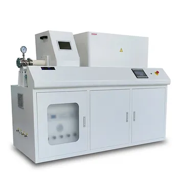
- Chemical Vapor Deposition CVD Equipment System Chamber Slide PECVD Tube Furnace with Liquid Gasifier PECVD Machine
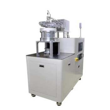
- Microwave Plasma Chemical Vapor Deposition MPCVD Machine System Reactor for Lab and Diamond Growth
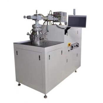
- Cylindrical Resonator MPCVD Machine System Reactor for Microwave Plasma Chemical Vapor Deposition and Lab Diamond Growth
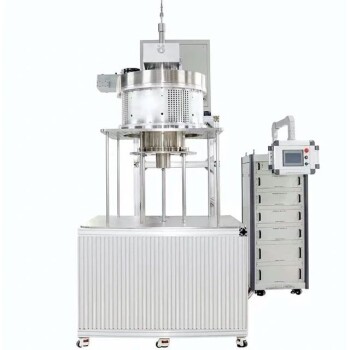
- 915MHz MPCVD Diamond Machine Microwave Plasma Chemical Vapor Deposition System Reactor
- RF PECVD System Radio Frequency Plasma-Enhanced Chemical Vapor Deposition RF PECVD
People Also Ask
- What are the advantages of chemical vapor deposition? Achieve Superior Thin Films for Your Lab
- What types of substrates are used in CVD to facilitate graphene films? Optimize Graphene Growth with the Right Catalyst
- What is the chemical vapor deposition growth process? Build Superior Thin Films from the Atom Up
- How expensive is chemical vapor deposition? Understanding the True Cost of High-Performance Coating
- Why is Chemical Vapor Deposition (CVD) equipment uniquely suited for constructing hierarchical superhydrophobic structures?