The bridge to semiconductor efficiency.
A tube annealing furnace is required for Cadmium Sulfide (CdS) post-treatment to facilitate short-time thermal treatment—typically around 500 °C—which induces recrystallization and eliminates internal stresses. This process is fundamental for improving the film's crystalline quality and optimizing the heterojunction interface between the CdS buffer layer and the subsequent absorber layer. Without this controlled thermal energy, the film remains plagued by structural defects that severely limit the efficiency of the final photovoltaic device.
Core Takeaway: The tube annealing furnace transforms a raw, as-deposited CdS film into a high-performance semiconductor by driving atomic rearrangement and grain growth. This thermal activation is the primary method for reducing non-radiative recombination and ensuring a high-quality electronic bond at the heterojunction.
Enhancing Structural Integrity and Crystallinity
Promoting Recrystallization and Grain Growth
Thermal energy provided by the furnace drives the transition of CdS from an amorphous or weakly crystalline state to a highly ordered hexagonal crystalline structure. This growth increases the grain size, which reduces the number of grain boundaries and effectively lowers the resistance to charge carrier flow.
Elimination of Internal Stress
The deposition process often leaves thin films with significant lattice distortion and internal stresses. High-temperature annealing allows for atomic rearrangement, which relaxes these stresses and creates a more stable, durable film layer that is less prone to mechanical failure or electronic instability.
Reduction of Structural Defects
By facilitating atomic movement, the furnace helps "heal" structural defects introduced during deposition. This reduction in defects is critical for adjusting the bandgap and ensuring the electrical characteristics of the film meet the rigorous requirements of semiconductor applications.
Optimizing the Heterojunction Interface
Passivation of Grain Boundary Defects
When used in conjunction with chemical treatments like Cadmium Chloride (CdCl2), the furnace provides the uniform energy needed to drive chlorine atoms into the CdS surface. This interaction passivates defect states at grain boundaries, which effectively inhibits non-radiative recombination and boosts the open-circuit voltage of the solar cell.
Improving Interface Bonding Strength
The thermal treatment enhances the interface bonding strength between the CdS buffer and absorber layers, such as CZTS or antimony-based materials. A stronger, cleaner bond at this interface is essential for efficient electron transport and long-term device stability.
Activation of Internal Dopants
For specialized films, the annealing furnace activates internal dopants (such as silver) and linking molecules. This activation is necessary to fine-tune the electrical conductivity and carrier mobility of the CdS layer for specific high-performance applications.
Critical Environmental Control
Atmospheric Isolation and Purity
Tube furnaces allow for precise control of the environment, often utilizing inert gases like Nitrogen or Argon. This isolation prevents oxidation of the thin films at high temperatures, ensuring that the chemical composition of the CdS remains pure.
Desorption of Impurities
The high-temperature environment promotes the desorption of moisture and volatile impurity molecules from the film surface. Removing these contaminants is vital for improving the contact quality between the CdS and the metal electrodes, which significantly increases the output current.
Understanding the Trade-offs
Temperature Sensitivity vs. Material Sublimation
While high temperatures are necessary for recrystallization, exceeding the optimal threshold can lead to the sublimation of the thin film or unwanted inter-diffusion. Finding the precise "thermal window"—often around 500 °C for CdS—is a delicate balance between improving crystallinity and maintaining film thickness.
Atmosphere Composition Risks
Using a mixed atmosphere, such as Argon-Hydrogen, can enhance impurity removal but introduces complexity in gas handling. If the atmosphere is not perfectly controlled, it can lead to unintended chemical reactions that alter the semiconductor’s optoelectronic properties.
How to Apply This to Your Project
When selecting a furnace protocol for CdS post-treatment, your specific device goals should dictate the parameters.
- If your primary focus is Maximum Conversion Efficiency: Prioritize a high-temperature (~500 °C) short-time thermal treatment to maximize grain growth and minimize interface recombination.
- If your primary focus is Long-term Device Stability: Focus on a controlled Nitrogen atmosphere to ensure complete stress relief and prevent any oxidative degradation of the film.
- If your primary focus is Electrical Conductivity: Incorporate dopant activation phases at lower temperatures (200-300 °C) to ensure internal reagents are properly integrated without damaging the film structure.
Mastering the thermal environment of a tube furnace is the definitive path to transforming raw thin films into scalable, high-efficiency semiconductor components.
Summary Table:
| Key Process | Impact on CdS Thin Film | Primary Performance Benefit |
|---|---|---|
| Recrystallization | Transition to hexagonal crystalline structure | Increased grain size & lower resistance |
| Stress Relief | Atomic rearrangement & lattice relaxation | Improved mechanical & electronic stability |
| Interface Passivation | Reduction of grain boundary defects | Lower recombination & higher open-circuit voltage |
| Atmospheric Control | Isolation from oxygen (Nitrogen/Argon) | High chemical purity & prevention of oxidation |
| Impurity Desorption | Removal of moisture & volatile molecules | Enhanced contact quality with metal electrodes |
Elevate Your Semiconductor Research with KINTEK Precision
Achieving high-efficiency CdS thin films requires absolute control over thermal parameters and atmospheric purity. KINTEK specializes in high-performance laboratory equipment designed to meet the rigorous demands of material science.
Our extensive portfolio includes:
- High-Temperature Furnaces: Precision tube, muffle, vacuum, and atmosphere furnaces tailored for semiconductor annealing.
- Advanced Systems: CVD, PECVD, and MPCVD systems for thin-film deposition and growth.
- Sample Preparation: Crushing, milling, and high-pressure hydraulic presses for pellet and material processing.
- Specialized Lab Tools: High-temperature reactors, autoclaves, and essential consumables like PTFE and ceramics.
Whether you are optimizing heterojunction interfaces or scaling up photovoltaic production, KINTEK provides the reliable technology and expert support you need to succeed.
Ready to upgrade your lab’s thermal capabilities? Contact KINTEK today for a custom solution!
References
- Huafei Guo, Jianning Ding. Enhancement in the Efficiency of Sb<sub>2</sub>Se<sub>3</sub> Solar Cells by Triple Function of Lithium Hydroxide Modified at the Back Contact Interface. DOI: 10.1002/advs.202304246
This article is also based on technical information from Kintek Solution Knowledge Base .
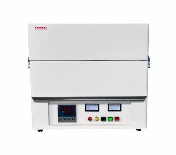
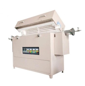
Related Products
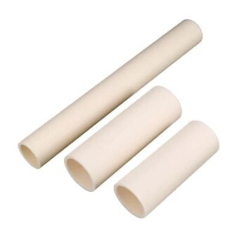
- High Temperature Alumina (Al2O3) Furnace Tube for Engineering Advanced Fine Ceramics
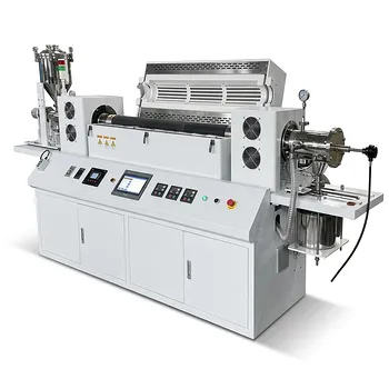
- Vacuum Sealed Continuous Working Rotary Tube Furnace Rotating Tube Furnace
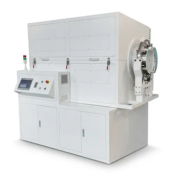
- Laboratory Vacuum Tilt Rotary Tube Furnace Rotating Tube Furnace
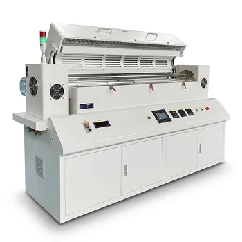
- 1200℃ Split Tube Furnace with Quartz Tube Laboratory Tubular Furnace
- Rotary Tube Furnace Split Multi Heating Zone Rotating Tube Furnace
People Also Ask
- Why is a high-temperature tube furnace core to carbon black recovery? Master Precision Pyrolysis & Material Regeneration
- What role does a high-alumina furnace tube play in high-temperature nickel slag reduction? Ensure 1400°C Precision
- How does a high-temperature tube ceramic furnace ensure stable molten salt carbon capture? Achieve Precise Thermal Cycles
- How do you clean an alumina tube furnace? Extend Tube Life with Proper Maintenance
- What is the process of alumina tube manufacturing? From Powder to High-Performance Ceramic