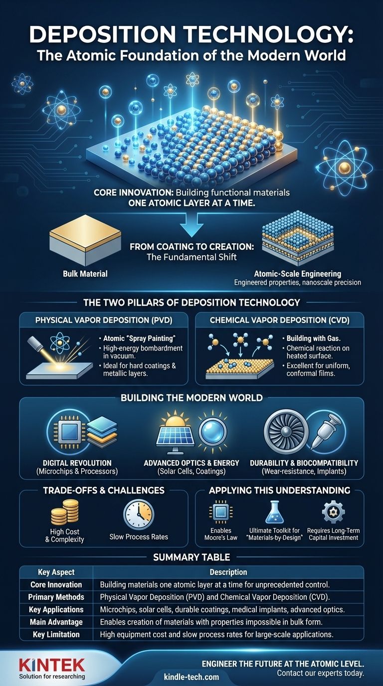
At its core, deposition technology is a scientific advancement that allows us to build functional materials one layer of atoms at a time. Its power lies in the unprecedented control it provides over a material's structure at the nanoscale. This atomic-level precision enables the creation of thin films with specific optical, electrical, or mechanical properties that are impossible to achieve with bulk materials, forming the physical foundation for virtually all modern electronics and advanced coatings.
The true revolution of deposition is not just in applying coatings, but in constructing entirely new materials from the ground up. It shifted our capabilities from simply working with existing materials to engineering new ones with properties designed for a specific purpose.
From Coating to Creation: The Fundamental Shift
The importance of deposition technology comes from a fundamental change in how we think about and create materials. We moved beyond the limitations of naturally occurring bulk substances into the realm of atomic-scale engineering.
The Power of the Nanoscale
Materials behave differently at the nanoscale (billionths of a meter). By creating films that are only a few hundred or even a few dozen atoms thick, we can manipulate properties like conductivity, transparency, and hardness in ways that are not possible otherwise.
Deposition is the essential tool that gives us access to this nanoscale world, allowing us to harness these unique properties for practical applications.
Unprecedented Precision and Purity
Modern technologies, especially semiconductors, demand near-perfect materials. Deposition processes occur in high-vacuum environments, which prevents contamination and results in films of exceptionally high purity.
Furthermore, these techniques allow for thickness control with sub-nanometer precision. This level of control is non-negotiable for building the complex, multi-layered structures found in a computer chip.
The Two Pillars of Deposition Technology
While there are many specific methods, most fall into two major categories: Physical Vapor Deposition (PVD) and Chemical Vapor Deposition (CVD). Understanding them helps clarify how this technology works.
Physical Vapor Deposition (PVD)
Think of PVD as a form of atomic-level spray painting. In a vacuum, a solid source material (a "target") is bombarded with energy, causing atoms to be ejected or "sputtered" off. These vaporized atoms then travel through the vacuum and condense onto a substrate, forming a thin, uniform film.
This method is widely used for creating hard, wear-resistant coatings on cutting tools, durable decorative finishes on watches, and metallic layers inside microchips.
Chemical Vapor Deposition (CVD)
CVD is more like building a structure with gas. Precursor gases are introduced into a reaction chamber containing a heated substrate. The heat causes a chemical reaction on the substrate's surface, leaving behind a solid film of the desired material.
CVD excels at creating highly uniform films that can conform perfectly to complex, three-dimensional shapes. It is critical for producing the high-purity silicon and insulating layers that form the basis of transistors in integrated circuits.
How Deposition Builds the Modern World
The applications of deposition are so widespread that it's difficult to imagine modern life without them. It is not an isolated technology but an enabling platform for countless other advancements.
Enabling the Digital Revolution
Microchips are the most profound example. A modern processor contains billions of transistors, each built from dozens of meticulously stacked layers of conductive, insulating, and semiconducting films. Every one of these layers is applied using a deposition technique. Without it, there would be no computers, smartphones, or data centers.
Advanced Optics and Energy
Anti-reflective coatings on eyeglasses and camera lenses are created with deposition to control how light is transmitted. Low-emissivity (Low-E) coatings on modern windows use deposited metallic films to reflect heat, dramatically improving energy efficiency. High-efficiency solar cells rely on multiple deposited layers to optimize light absorption and electron conversion.
Durability and Biocompatibility
The blades inside a jet engine are coated with advanced ceramic films using deposition to withstand extreme temperatures and prevent corrosion. In medicine, biocompatible coatings are deposited onto medical implants like artificial hips and stents to ensure they are not rejected by the body.
Understanding the Trade-offs and Challenges
Despite its incredible power, deposition technology is not without its limitations. Its precision comes at a cost.
High Cost and Complexity
Deposition systems are highly complex and expensive pieces of equipment. They require ultra-high vacuum chambers, sophisticated power supplies, and precise control systems, representing a significant capital investment.
Slow Process Rates
Building something atom by atom is, by its nature, a slow process. While perfect for tiny, high-value components like microprocessors, the slow deposition rate can make it impractical for coating very large objects quickly and cheaply.
Material and Substrate Constraints
Successfully depositing a film requires careful engineering. Issues like poor adhesion between the film and the substrate, or internal stresses that cause the film to crack, are constant challenges that require deep materials science expertise to overcome.
Applying This Understanding
Grasping the role of deposition technology provides a foundational insight into how modern hardware is created and where future innovation lies.
- If your primary focus is on electronics or computer science: Understand that deposition is the physical manufacturing process that has enabled Moore's Law, allowing for the exponential growth in computing power for over 50 years.
- If your primary focus is on materials science or engineering: View deposition as the ultimate toolkit for designing "materials-by-design," creating engineered surfaces and metamaterials with properties not found in nature.
- If your primary focus is on business or technology strategy: Recognize that advancements in hardware often depend on breakthroughs in deposition, and that leadership in this area requires immense, long-term capital investment in manufacturing.
Ultimately, deposition technology is revolutionary because it provides humanity with the ability to engineer our physical world from the atoms up.
Summary Table:
| Key Aspect | Description |
|---|---|
| Core Innovation | Building materials one atomic layer at a time for unprecedented control. |
| Primary Methods | Physical Vapor Deposition (PVD) and Chemical Vapor Deposition (CVD). |
| Key Applications | Microchips, solar cells, durable coatings, medical implants, advanced optics. |
| Main Advantage | Enables creation of materials with properties impossible in bulk form. |
| Key Limitation | High equipment cost and slow process rates for large-scale applications. |
Ready to engineer the future at the atomic level?
Deposition technology is the cornerstone of modern material science and electronics. Whether you are developing next-generation semiconductors, durable coatings, or advanced optical components, having the right equipment is critical.
KINTEK specializes in high-precision lab equipment and consumables, serving the exacting needs of laboratories and R&D departments. Our expertise in deposition technologies can help you achieve the purity, precision, and performance your projects demand.
Contact our experts today to discuss how KINTEK's solutions can accelerate your material engineering breakthroughs.
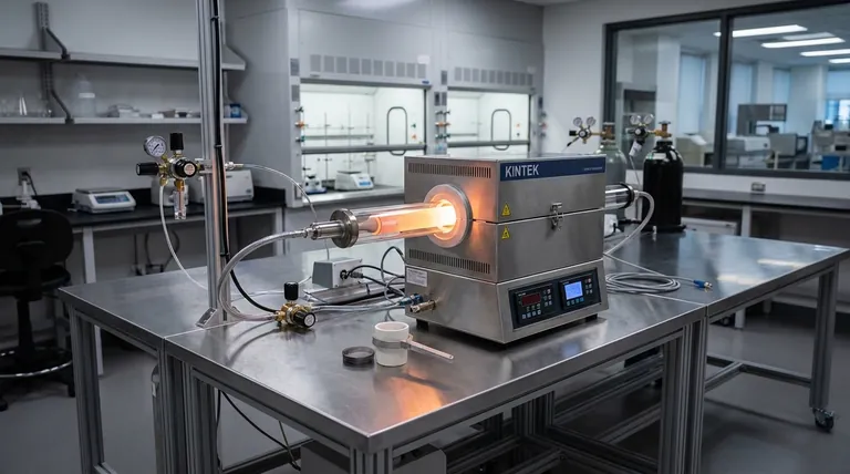
Visual Guide
Related Products
- Chemical Vapor Deposition CVD Equipment System Chamber Slide PECVD Tube Furnace with Liquid Gasifier PECVD Machine
- RF PECVD System Radio Frequency Plasma-Enhanced Chemical Vapor Deposition RF PECVD
- Inclined Rotary Plasma Enhanced Chemical Vapor Deposition PECVD Equipment Tube Furnace Machine
- Inclined Rotary Plasma Enhanced Chemical Vapor Deposition PECVD Equipment Tube Furnace Machine
- Electron Beam Evaporation Coating Oxygen-Free Copper Crucible and Evaporation Boat
People Also Ask
- What is the chemical vapor deposition growth process? Build Superior Thin Films from the Atom Up
- What is plasma enhanced chemical vapor deposition PECVD equipment? A Guide to Low-Temperature Thin Film Deposition
- Why is Chemical Vapor Deposition (CVD) equipment uniquely suited for constructing hierarchical superhydrophobic structures?
- What are the core advantages of PE-CVD in OLED encapsulation? Protect Sensitive Layers with Low-Temp Film Deposition
- How are carbon nanotubes grown? Master Scalable Production with Chemical Vapor Deposition


