Depositing a thin film is a process of applying a material layer, ranging from a few nanometers to several micrometers in thickness, onto a surface or "substrate." The methods for achieving this are broadly divided into two fundamental categories: Physical Vapor Deposition (PVD) and Chemical Vapor Deposition (CVD). These two families encompass a range of techniques, from sputtering and evaporation to atomic-level chemical reactions.
The core decision in thin film deposition is not just what method to use, but why. The choice between a physical process (PVD) and a chemical one (CVD) is determined entirely by your application's specific requirements for film purity, conformity, temperature tolerance, and precision.
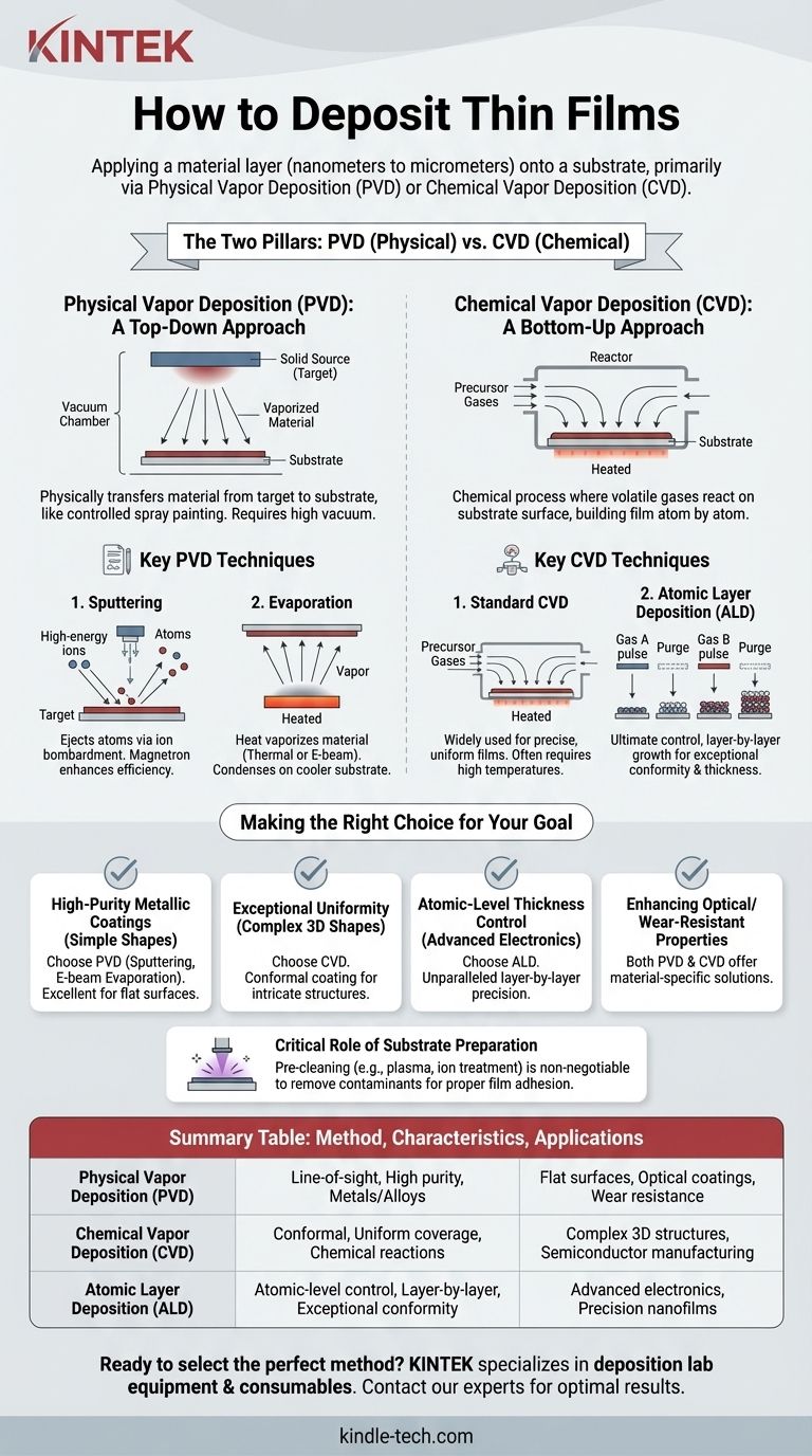
The Two Pillars of Deposition: PVD vs. CVD
Understanding the fundamental difference between physical and chemical deposition is the first step toward selecting the correct technique. They represent two distinct philosophies for building a film on a substrate.
Physical Vapor Deposition (PVD): A "Top-Down" Approach
PVD methods involve physically transferring material from a solid source (called a "target") to the substrate within a vacuum chamber. Think of this as a highly controlled, molecular-level form of spray painting.
The material is vaporized from the target and travels in a straight line, condensing onto the substrate.
Key PVD Techniques
Sputtering is a process where a target is bombarded with high-energy ions (typically from a gas like Argon). This collision ejects, or "sputters," atoms from the target, which then deposit onto the substrate. Magnetron sputtering uses powerful magnets to improve the efficiency of this process.
Evaporation involves heating a material in a high vacuum until it vaporizes. The vapor then rises and condenses on the cooler substrate. This can be done through thermal heating (thermal evaporation) or by using a focused stream of electrons (e-beam evaporation).
Chemical Vapor Deposition (CVD): A "Bottom-Up" Approach
CVD is a chemical process where the substrate is exposed to one or more volatile precursor gases. These gases react or decompose on the substrate's surface, creating the desired solid film.
This is less like spraying and more like building a structure atom by atom using controlled chemical reactions.
Key CVD Techniques
Standard CVD is widely used in the semiconductor industry for its ability to produce highly precise and uniform films. It often requires high temperatures to drive the necessary chemical reactions on the substrate surface.
Atomic Layer Deposition (ALD) is an advanced form of CVD that offers the ultimate control. It uses a sequence of self-limiting chemical reactions to deposit a single atomic layer at a time. This layer-by-layer approach produces films with exceptional conformity and thickness control.
Understanding the Trade-offs
Neither PVD nor CVD is universally superior. The optimal choice is a function of the material, the substrate, and the desired outcome.
When to Choose PVD
PVD is often preferred for depositing high-purity coatings of metals, alloys, and certain ceramics. Because it's a line-of-sight process, it's excellent for coating flat surfaces.
Techniques like sputtering are highly versatile and can deposit a vast range of materials, including those with very high melting points that are difficult to evaporate.
When to Choose CVD
CVD excels where uniformity and conformity are critical. Because the precursor gases can flow around complex shapes, CVD can evenly coat intricate 3D structures and trenches, something PVD struggles with.
This is why CVD and its subtype, ALD, are dominant in modern semiconductor manufacturing, where flawless coverage over complex transistor architectures is essential.
The Critical Role of Substrate Preparation
No deposition technique will succeed on a contaminated surface. Pre-cleaning is a non-negotiable step to ensure proper film adhesion and quality.
Methods like plasma treatment or ion source cleaning are used to remove microscopic contaminants such as hydrocarbons, moisture, or unwanted native oxide layers from the substrate right before it enters the deposition chamber.
Making the Right Choice for Your Goal
Your application dictates the technology. Base your decision on the primary requirement you need to fulfill.
- If your primary focus is high-purity metallic coatings on a simple surface: PVD methods like sputtering or e-beam evaporation are your most direct and effective choice.
- If your primary focus is exceptional uniformity on complex 3D shapes: CVD is superior due to its ability to conformally coat all surfaces.
- If your primary focus is atomic-level thickness control for advanced electronics: Atomic Layer Deposition (ALD), a precise type of CVD, offers unparalleled, layer-by-layer control.
- If your primary focus is enhancing optical or wear-resistant properties: Both PVD and CVD offer a wide range of material solutions, and the choice will depend on the specific material and substrate involved.
Understanding these fundamental principles allows you to select the precise deposition technique your project demands.
Summary Table:
| Deposition Method | Key Characteristics | Primary Applications |
|---|---|---|
| Physical Vapor Deposition (PVD) | Line-of-sight process, high-purity coatings, works with metals/alloys | Flat surfaces, optical coatings, wear-resistant layers |
| Chemical Vapor Deposition (CVD) | Conformal coating, uniform coverage, chemical reactions on surface | Complex 3D structures, semiconductor manufacturing |
| Atomic Layer Deposition (ALD) | Atomic-level control, layer-by-layer growth, exceptional conformity | Advanced electronics, precision nanofilms |
Ready to select the perfect thin film deposition method for your project? KINTEK specializes in lab equipment and consumables for all your deposition needs, from sputtering targets to CVD precursors. Our experts can help you choose the right technique for optimal film purity, conformity, and performance. Contact us today to discuss your specific application requirements!
Visual Guide
Related Products
- Aluminized Ceramic Evaporation Boat for Thin Film Deposition
- Tungsten Evaporation Boat for Thin Film Deposition
- Electron Beam Evaporation Coating Oxygen-Free Copper Crucible and Evaporation Boat
- Molybdenum Tungsten Tantalum Evaporation Boat for High Temperature Applications
- Vacuum Hot Press Furnace Machine for Lamination and Heating
People Also Ask
- Why is an alumina boat selected for catalyst precursors? Ensure Sample Purity at 1000 °C
- What are the alternatives to sputtering? Choose the Right Thin Film Deposition Method
- What are the applications of thin films deposition? Unlock New Possibilities for Your Materials
- What is the chemical method for thin film deposition? Build Films from the Molecular Level Up
- Why are high-purity ceramic boats used for lignin activation? Ensure Purity & Thermal Stability


