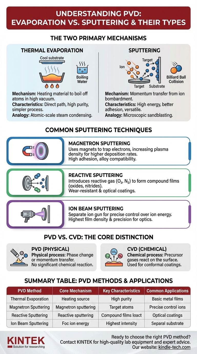
To be precise, Physical Vapor Deposition (PVD) is not defined by a specific number of types but is best understood as two primary, fundamentally different mechanisms: Evaporation and Sputtering. Within each of these categories, especially sputtering, there are numerous specialized techniques developed to control the properties of the final thin film.
The critical insight is not to memorize a list of PVD methods, but to understand the core distinction between them. The choice between evaporating a material (like boiling water) and sputtering it (like sandblasting with ions) is the most important decision, as it dictates the energy, adhesion, and quality of the deposited film.
The Two Pillars of PVD: Evaporation vs. Sputtering
At its core, all PVD processes occur in a vacuum and involve physically moving material from a source (the "target") to a destination (the "substrate") without a chemical reaction. The method used to dislodge and transport those atoms defines the process.
Thermal Evaporation: The Direct Path
This is the conceptually simplest form of PVD. A source material is heated in a high vacuum chamber until its atoms gain enough thermal energy to boil off, travel through the vacuum, and condense onto the cooler substrate.
Think of it as the atomic-scale equivalent of boiling water and seeing steam condense on a cool mirror.
Sputtering: The Billiard Ball Collision
Sputtering is a momentum-transfer process. High-energy ions, typically from an inert gas like Argon, are accelerated to strike a target material.
This collision physically knocks out, or "sputters," atoms from the target, which then deposit onto the substrate. It's less like boiling and more like a microscopic sandblasting where the "sand" is individual ions and the ejected material forms the coating.
Common Sputtering Techniques
Sputtering is highly versatile and is the basis for many advanced industrial PVD methods. The variations focus on improving the efficiency and control of the ion bombardment.
Magnetron Sputtering
This is one of the most widely used PVD techniques. It uses powerful magnets behind the target to trap electrons near the target's surface.
These trapped electrons increase the ionization efficiency of the sputtering gas (like Argon), creating a dense plasma. This leads to a much higher sputtering rate and faster deposition compared to basic sputtering.
Reactive Sputtering
In this method, a reactive gas like oxygen or nitrogen is intentionally introduced into the vacuum chamber along with the inert sputtering gas.
The sputtered metal atoms react with this gas on their way to the substrate, or on the substrate itself, to form a compound film. This is how materials like titanium nitride (a hard coating) or silicon dioxide (an insulator) are created.
Ion Beam Sputtering
Ion beam sputtering offers the highest level of control. It uses a separate ion source or "gun" to generate and accelerate a well-controlled beam of ions toward the target.
This decouples the plasma generation from the target, allowing for independent control over ion energy and flux. The result is often the highest quality, densest, and most precise films, which are critical for applications like optical coatings.
Common Pitfalls to Avoid: PVD vs. CVD
It is crucial to distinguish PVD from its counterpart, Chemical Vapor Deposition (CVD), as they are often discussed together but are fundamentally different.
The Core Distinction
PVD is a physical process. It involves phase changes (solid to gas to solid) or momentum transfer (sputtering). No significant chemical reactions occur.
CVD is a chemical process. It uses precursor gases that react on the substrate surface at high temperatures to form the desired film, leaving behind volatile byproducts that are pumped away. The references mention methods like AACVD and DLICVD, which are both types of CVD, not PVD.
Why It Matters
Choosing PVD is often driven by a need for lower deposition temperatures (protecting the substrate), depositing pure metals or complex alloys, or achieving very high density and adhesion, which is characteristic of sputtering processes.
CVD excels at creating highly uniform (conformal) coatings over complex 3D shapes and is often used for specific semiconductor or crystalline material growth.
Making the Right Choice for Your Goal
Selecting the correct deposition method requires understanding your final objective for the thin film.
- If your primary focus is high purity and simplicity for a basic metal film: Thermal Evaporation is often the most direct and cost-effective method.
- If your primary focus is strong adhesion, coating a complex alloy, or high deposition rates: Magnetron Sputtering is the industry workhorse and the most likely starting point.
- If your primary focus is creating a ceramic or compound coating (e.g., an oxide or nitride): Reactive Sputtering is the designated technique.
- If your primary focus is ultimate precision, density, and low-loss films for optics or electronics: Ion Beam Sputtering provides the highest degree of process control.
Ultimately, understanding the mechanism—boiling or bombarding—is the key to selecting the right tool for your material and application.
Summary Table:
| PVD Method | Core Mechanism | Key Characteristics | Common Applications |
|---|---|---|---|
| Thermal Evaporation | Heating source material to vaporize atoms | High purity, simple process, lower adhesion | Basic metal films, OLEDs, research coatings |
| Magnetron Sputtering | Ion bombardment with magnetic plasma confinement | High deposition rates, strong adhesion, alloy compatibility | Decorative coatings, hard coatings, semiconductor metallization |
| Reactive Sputtering | Sputtering in reactive gas atmosphere (e.g., O₂, N₂) | Forms compound films (oxides, nitrides) | Wear-resistant coatings, optical films, barrier layers |
| Ion Beam Sputtering | Separate ion gun for precise bombardment | Highest film density, ultimate precision, low defect density | High-performance optics, precision electronics, research-grade films |
Ready to choose the right PVD method for your application?
At KINTEK, we specialize in providing high-quality lab equipment and consumables for all your Physical Vapor Deposition needs. Whether you're working with basic metal films or complex compound coatings, our experts can help you select the perfect solution for superior adhesion, precision, and performance.
Contact us today to discuss how our PVD solutions can enhance your laboratory's capabilities and achieve your thin film goals. Get in touch with our specialists now!
Visual Guide
Related Products
- Chemical Vapor Deposition CVD Equipment System Chamber Slide PECVD Tube Furnace with Liquid Gasifier PECVD Machine
- RF PECVD System Radio Frequency Plasma-Enhanced Chemical Vapor Deposition RF PECVD
- 915MHz MPCVD Diamond Machine Microwave Plasma Chemical Vapor Deposition System Reactor
- HFCVD Machine System Equipment for Drawing Die Nano-Diamond Coating
- Customer Made Versatile CVD Tube Furnace Chemical Vapor Deposition Chamber System Equipment
People Also Ask
- How are carbon nanotubes grown? Master Scalable Production with Chemical Vapor Deposition
- What types of substrates are used in CVD to facilitate graphene films? Optimize Graphene Growth with the Right Catalyst
- How expensive is chemical vapor deposition? Understanding the True Cost of High-Performance Coating
- What are the advantages of chemical vapor deposition? Achieve Superior Thin Films for Your Lab
- What is the chemical vapor deposition growth process? Build Superior Thin Films from the Atom Up


