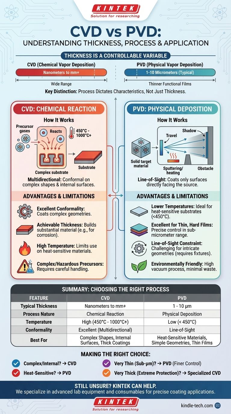
At its core, there is no fixed thickness for either coating. Both Chemical Vapor Deposition (CVD) and Physical Vapor Deposition (PVD) are processes whose thickness is a controllable variable. However, the nature of each process means PVD is typically used for thinner functional films (often 1-10 micrometers), while CVD can achieve a much wider range, from nanometers in electronics to several millimeters for bulk material growth.
The critical distinction is not a predefined thickness but how the underlying process—a chemical reaction for CVD versus a physical deposition for PVD—dictates the coating's characteristics, temperature requirements, and suitability for your specific component geometry.
The Fundamental Process: Chemical vs. Physical
Understanding the "how" behind each method is the key to choosing the right one. They are fundamentally different approaches to building a thin film.
How CVD Works: A Chemical Reaction
CVD involves introducing precursor gases into a high-temperature chamber.
These gases react on the surface of the substrate, forming a new solid material that grows layer by layer. Because the deposition happens from a gaseous state, it is multidirectional.
This allows the coating to form uniformly over complex shapes and even inside cavities, creating a highly conformal layer.
How PVD Works: A Physical Deposition
PVD begins with a solid material (a target) in a vacuum chamber.
This material is vaporized by physical means (like sputtering with ions or heating via thermal evaporation) and travels in a straight line to condense on the substrate.
This is a line-of-sight process. Only the surfaces directly facing the vapor source will be coated, much like spray paint.
Why Process Dictates Application
The differences in their core mechanics create distinct advantages and limitations that go far beyond just thickness.
Temperature and Substrate Sensitivity
CVD processes typically require very high temperatures (often 450°C to over 1000°C) to drive the necessary chemical reactions. This limits its use to materials that can withstand that heat without deforming or losing their temper.
PVD, in contrast, operates at much lower temperatures (generally below 450°C). This makes it the ideal choice for coating heat-sensitive substrates, such as hardened tool steels, plastics, or alloys that would be damaged by the CVD process.
Coating Conformality and Geometry
The multidirectional, gas-based nature of CVD makes it exceptionally good at coating complex shapes and internal surfaces uniformly.
PVD's line-of-sight limitation makes it challenging to coat intricate geometries. Areas not directly exposed to the vapor source will receive little to no coating, creating "shadows."
Achievable Thickness and Stress
While PVD is excellent for thin, hard coatings, building up very thick layers can lead to high internal stress, which may cause the coating to crack or delaminate.
CVD can often grow thicker, lower-stress coatings because the chemical bonding process can be more stable over greater depths. This makes it suitable for applications requiring substantial material buildup for corrosion or thermal barriers.
Understanding the Trade-offs
Neither technology is universally superior. The correct choice always depends on balancing the requirements of the application against the limitations of the process.
The CVD Compromise: High Heat and Gaseous Precursors
The primary drawback of CVD is its high operating temperature, which severely restricts the types of materials you can coat. It can also involve complex and sometimes hazardous precursor gases.
The PVD Limitation: Complex Shapes and Uniformity
The line-of-sight nature of PVD is its main constraint. Achieving uniform coverage on complex parts requires sophisticated fixtures and component rotation, which adds complexity and cost.
Environmental and Safety Factors
As a general rule, PVD is considered a more environmentally friendly process. It is a physical process that occurs in a high vacuum, producing very little waste. CVD can involve reactive byproducts that require careful handling and disposal.
Making the Right Choice for Your Application
Forget asking which is "thicker" and instead ask which process aligns with your material and geometry.
- If your primary focus is coating a complex part with internal channels or intricate features: CVD is the only way to ensure a truly uniform, conformal layer.
- If your primary focus is applying a hard, wear-resistant coating to a heat-sensitive material: PVD is almost certainly the correct and safer choice.
- If your primary focus is creating a very thin, high-purity film for optical or electronic applications: Both processes can work, but PVD often provides finer control in the sub-micrometer range.
- If your primary focus is building a very thick layer for extreme corrosion or thermal protection: Specialized CVD processes are often better suited for this goal.
Ultimately, your application's material, geometry, and required performance properties—not a preconceived notion of thickness—should guide your decision.
Summary Table:
| Feature | CVD (Chemical Vapor Deposition) | PVD (Physical Vapor Deposition) |
|---|---|---|
| Typical Thickness Range | Nanometers to several millimeters | 1 to 10 micrometers |
| Process Nature | Chemical reaction | Physical deposition |
| Temperature | High (450°C - 1000°C+) | Low (< 450°C) |
| Conformality | Excellent (multidirectional) | Line-of-sight |
| Best For | Complex shapes, internal surfaces, thick coatings | Heat-sensitive materials, simple geometries, thin films |
Still unsure whether CVD or PVD is right for your project?
At KINTEK, we specialize in providing advanced lab equipment and consumables for precise coating applications. Our experts can help you navigate the complexities of CVD and PVD processes to ensure optimal performance for your specific materials and component geometries.
Let us help you achieve superior coating results. Contact our team today to discuss your requirements and discover how KINTEK's solutions can enhance your laboratory's capabilities.
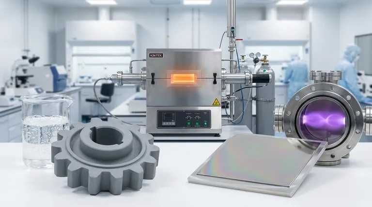
Visual Guide
Related Products
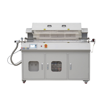
- Chemical Vapor Deposition CVD Equipment System Chamber Slide PECVD Tube Furnace with Liquid Gasifier PECVD Machine
- Inclined Rotary Plasma Enhanced Chemical Vapor Deposition PECVD Equipment Tube Furnace Machine
- RF PECVD System Radio Frequency Plasma-Enhanced Chemical Vapor Deposition RF PECVD
- Customer Made Versatile CVD Tube Furnace Chemical Vapor Deposition Chamber System Equipment
- Vacuum Hot Press Furnace Machine for Lamination and Heating
People Also Ask
- What are the advantages of PECVD over CVD? Achieve High-Quality Thin Films at Lower Temperatures
- What is the difference between thermal CVD and PECVD? Choose the Right Thin-Film Deposition Method
- Why is PECVD better than CVD? Achieve Superior Low-Temperature Thin Film Deposition
- How is PECVD different from CVD? Unlock Low-Temperature Thin Film Deposition
- What is the difference between CVD and PVD process? A Guide to Choosing the Right Coating Method