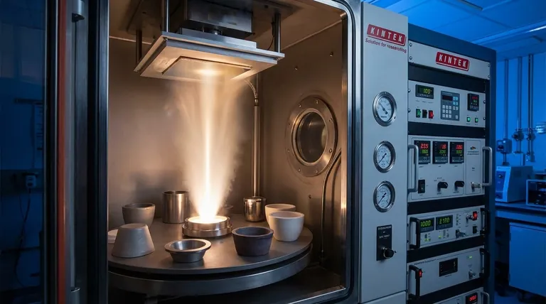
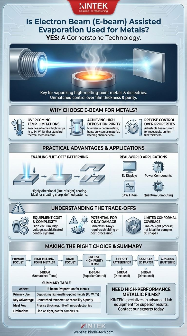
Yes, electron beam (e-beam) assisted evaporation is not only used for metals—it is a cornerstone technology for their deposition. This physical vapor deposition (PVD) method is specifically chosen for its ability to vaporize materials with very high melting points, including many metals and dielectrics that are impossible to process with simpler thermal techniques. Its high degree of control over film thickness and purity makes it indispensable for advanced applications.
E-beam evaporation is the preferred method for depositing high-melting-point metals or when precise control over film thickness and structure is paramount. It overcomes the temperature limitations of simpler thermal evaporation techniques, enabling the use of a wider range of high-performance materials.
Why Choose E-beam Evaporation for Metals?
The decision to use e-beam evaporation over other methods is driven by distinct technical advantages related to temperature, purity, and control.
Overcoming Temperature Limitations
Many technologically important metals, such as platinum, tungsten, and tantalum, have extremely high evaporation temperatures. Standard thermal evaporation, which uses a resistively heated boat or filament, simply cannot reach these temperatures effectively or without contaminating the film.
The e-beam process uses a high-energy beam of electrons to heat the source material directly and locally. This intense, focused energy can vaporize virtually any material, making it a highly versatile and capable tool.
Achieving High Deposition Purity
Because the electron beam heats only the source material in its crucible, the surrounding vacuum chamber components remain relatively cool. This minimizes outgassing and contamination from the equipment itself.
This results in a much purer deposited film compared to methods where a heating element is in close proximity to the source material.
Gaining Precise Control Over Film Properties
The deposition rate in an e-beam system can be controlled with exceptional precision by adjusting the beam's current. This allows for the creation of films with highly repeatable and uniform thickness, from a few angstroms to many microns.
This level of control is critical in applications like optical coatings and microelectronics, where film thickness directly impacts device performance.
The Practical Advantages of the E-beam Process
Beyond its fundamental capabilities, the nature of the e-beam process yields benefits for specific manufacturing techniques.
Enabling "Lift-Off" Patterning
E-beam evaporation is a line-of-sight process, meaning the evaporated material travels in a straight line from the source to the substrate. This results in a highly directional, or anisotropic, coating.
This property is ideal for a patterning technique called "lift-off," where a mask is applied to the substrate before deposition. The directional coating ensures clean edges with no material deposited on the sidewalls of the mask, allowing for easy removal and the creation of very sharp, well-defined patterns.
Real-World Applications
The precision and material versatility of e-beam evaporation are leveraged across many industries. You can find e-beam deposited metallic films in:
- Organic and inorganic electroluminescent (EL) displays
- Power pack components
- Surface acoustic wave (SAW) filters
- Components for watches and lithium-ion batteries
- Josephson junctions for quantum computing
Understanding the Trade-offs
No technology is without its limitations. Being a trusted advisor means presenting an objective view.
Equipment Complexity and Cost
E-beam evaporators are significantly more complex and expensive than standard thermal evaporators. They require a high-vacuum environment, high-voltage power supplies, and sophisticated control systems, leading to higher initial investment and maintenance costs.
Potential for X-ray Damage
The high-energy electron beam generates X-rays as a byproduct when it strikes the source material. These X-rays can potentially damage sensitive substrates or electronic devices. While often manageable with shielding or post-processing, it is a critical factor for certain applications.
Limited Conformal Coverage
The same line-of-sight property that is an advantage for lift-off is a disadvantage for coating complex, three-dimensional shapes. The process cannot easily coat "shadowed" areas, leading to non-uniform coverage on non-flat surfaces. For such applications, a more conformal technique like sputtering is often preferred.
Making the Right Choice for Your Metal
To determine if e-beam evaporation is the correct approach, consider your primary objective.
- If your primary focus is depositing high-melting-point metals (e.g., platinum, tungsten, titanium): E-beam is often the only practical evaporation method due to its unmatched temperature capabilities.
- If your primary focus is creating precise, high-purity films for electronics or optics: The fine control over deposition rate and the inherently clean process make e-beam a superior choice.
- If your primary focus is patterning using a lift-off process: The directional, line-of-sight deposition of e-beam is perfectly suited for creating sharp, well-defined features.
- If your primary focus is coating complex 3D parts or minimizing equipment cost: You should evaluate alternative methods like sputtering for coverage or standard thermal evaporation for lower-temperature metals.
Ultimately, understanding these capabilities allows you to select e-beam evaporation not just as a method, but as the right tool for achieving high-performance metallic films.
Summary Table:
| Aspect | E-beam Evaporation for Metals |
|---|---|
| Primary Use | Depositing high-melting-point metals (e.g., Pt, W, Ta) |
| Key Advantage | Unmatched temperature capability and high film purity |
| Ideal For | Precise film thickness control, lift-off patterning, microelectronics |
| Limitation | Line-of-sight process; not ideal for complex 3D coatings |
Need to deposit high-performance metallic films with precision and purity? KINTEK specializes in advanced lab equipment, including electron beam evaporation systems, to meet the demanding needs of research and production laboratories. Our solutions are designed to help you achieve superior results with high-melting-point metals and delicate substrates. Contact our experts today to discuss how we can support your specific application and enhance your laboratory's capabilities.
Visual Guide
Related Products
- Electron Beam Evaporation Coating Tungsten Crucible and Molybdenum Crucible for High Temperature Applications
- Electron Beam Evaporation Coating Oxygen-Free Copper Crucible and Evaporation Boat
- Electron Beam Evaporation Coating Gold Plating Tungsten Molybdenum Crucible for Evaporation
- Electron Beam Evaporation Coating Conductive Boron Nitride Crucible BN Crucible
- E Beam Crucibles Electron Gun Beam Crucible for Evaporation
People Also Ask
- What is the deposition rate of e-beam evaporation? Control Thin Film Quality and Speed
- What is the voltage of e-beam evaporation? Achieve Precise Thin-Film Deposition
- What is e-beam evaporation? Achieve High-Purity Thin Film Deposition for Your Lab
- What is e-beam evaporation used for? Precision Coating for Optics, Aerospace & Electronics
- What is the container that holds the metal source material called in e-beam evaporation? Ensure Purity and Quality in Your Thin-Film Deposition


