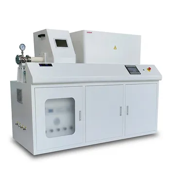
Chemical Vapor Deposition (CVD) equipment offers superior precision by enabling atomic-level control over the growth of platinum nanoparticles. It ensures high uniformity and discrete particle distribution, particularly when modifying complex three-dimensional titanium dioxide (TiO2) nanostructures.
Core Takeaway: The primary value of CVD lies in its ability to create a precise, efficient Schottky barrier. This significantly enhances the separation of photo-generated electrons and holes, resulting in superior performance compared to traditional deposition methods.
The Mechanics of Deposition Control
Atomic-Level Growth
CVD equipment provides the capability to control growth at the atomic level. This precision is essential when modifying sensitive materials like titanium dioxide single-crystal thin films.
High Uniformity
Unlike less precise methods, CVD ensures that platinum particles are distributed with high uniformity. This prevents the formation of uneven clusters that could degrade material performance.
Discrete Distribution
The system allows for discrete particle placement. This means the platinum remains as distinct nanoparticles rather than merging into an unintentional continuous film.
Structural Integrity on Nanoscale Features
3D Nanostructure Coverage
CVD is particularly advantageous for coating three-dimensional nanostructures. Its gas-phase nature allows it to penetrate and coat complex geometries that line-of-sight methods might miss.
Modifying Single-Crystal Films
The equipment is specifically optimized for modifying single-crystal thin films. It allows for the introduction of metal particles without compromising the underlying crystal structure.
Optimizing Electronic Performance
Creating the Schottky Barrier
The precise deposition of platinum creates an efficient Schottky barrier at the interface with the titanium dioxide. This barrier is the fundamental mechanism that regulates electron flow between the metal and the semiconductor.
Improving Charge Separation
A well-formed Schottky barrier significantly improves the separation efficiency of photo-generated electrons and holes.
Reducing Recombination
By enhancing charge separation, the system prevents electrons and holes from recombining too quickly. This directly translates to higher efficiency in photochemical applications.
Understanding the Trade-offs
The Limitations of Traditional Methods
The primary trade-off to consider is the performance gap between CVD and traditional deposition methods.
Efficiency Loss
Traditional methods often fail to achieve the atomic precision required for an optimal Schottky barrier. This results in lower separation efficiency of photo-generated charges.
Lack of Conformal Coating
Standard techniques may struggle to coat three-dimensional structures uniformly. This can lead to gaps in coverage and inconsistent electronic properties across the device.
Making the Right Choice for Your Goal
- If your primary focus is maximum efficiency: Prioritize CVD to ensure the formation of a high-quality Schottky barrier for optimal electron-hole separation.
- If your primary focus is complex geometry: Use CVD to guarantee uniform, discrete particle distribution across three-dimensional nanostructures.
Precise control over particle growth is the defining factor in maximizing the electronic capabilities of platinum-modified titanium dioxide.
Summary Table:
| Feature | CVD Method Advantage | Impact on Material Performance |
|---|---|---|
| Deposition Control | Atomic-level precision | Enables discrete, uniform nanoparticle growth |
| Structural Coverage | Gas-phase penetration | Seamless coating of 3D TiO2 nanostructures |
| Electronic Interface | Schottky barrier creation | Enhanced separation of photo-generated electrons |
| System Efficiency | Reduced charge recombination | Maximizes performance in photochemical applications |
Elevate Your Nanotechnology Research with KINTEK
Precision at the atomic level is the difference between average results and groundbreaking discoveries. At KINTEK, we specialize in high-performance laboratory equipment, including advanced CVD and PECVD systems designed for the meticulous modification of nanostructures like TiO2.
Whether you are developing high-efficiency photocatalysts or advanced battery technologies, our comprehensive range of high-temperature furnaces, crushing systems, and specialized reactors ensures your research achieves maximum uniformity and electronic efficiency.
Ready to optimize your deposition process? Contact our experts today to find the perfect CVD solution for your laboratory!
References
- Samar Al Jitan, Corrado Garlisi. Synthesis and Surface Modification of TiO2-Based Photocatalysts for the Conversion of CO2. DOI: 10.3390/catal10020227
This article is also based on technical information from Kintek Solution Knowledge Base .
Related Products
- Chemical Vapor Deposition CVD Equipment System Chamber Slide PECVD Tube Furnace with Liquid Gasifier PECVD Machine
- HFCVD Machine System Equipment for Drawing Die Nano-Diamond Coating
- Multi Heating Zones CVD Tube Furnace Machine Chemical Vapor Deposition Chamber System Equipment
- CVD Diamond Dressing Tools for Precision Applications
- CVD Diamond Domes for Industrial and Scientific Applications
People Also Ask
- What are the core advantages of PE-CVD in OLED encapsulation? Protect Sensitive Layers with Low-Temp Film Deposition
- What is plasma enhanced chemical vapor deposition PECVD equipment? A Guide to Low-Temperature Thin Film Deposition
- How expensive is chemical vapor deposition? Understanding the True Cost of High-Performance Coating
- How are carbon nanotubes grown? Master Scalable Production with Chemical Vapor Deposition
- What types of substrates are used in CVD to facilitate graphene films? Optimize Graphene Growth with the Right Catalyst
