In the field of materials science, "external chemical vapor deposition" is not a standard, formally defined category. Instead, the term likely refers to CVD processes where the primary energy source or the initial decomposition of precursor gases occurs physically separate from, or "external" to, the substrate onto which the thin film is being deposited.
The core idea behind the "external CVD" concept is about control: separating the energy source or gas activation zone from the deposition zone. This contrasts with "internal" processes where the substrate itself might be the primary source of heat or be directly immersed in the energy field, like a plasma.
Deconstructing "External CVD": The Likely Interpretations
While not a formal classification, the term "external CVD" can be understood through two primary technical concepts. This distinction helps clarify the intent behind process design.
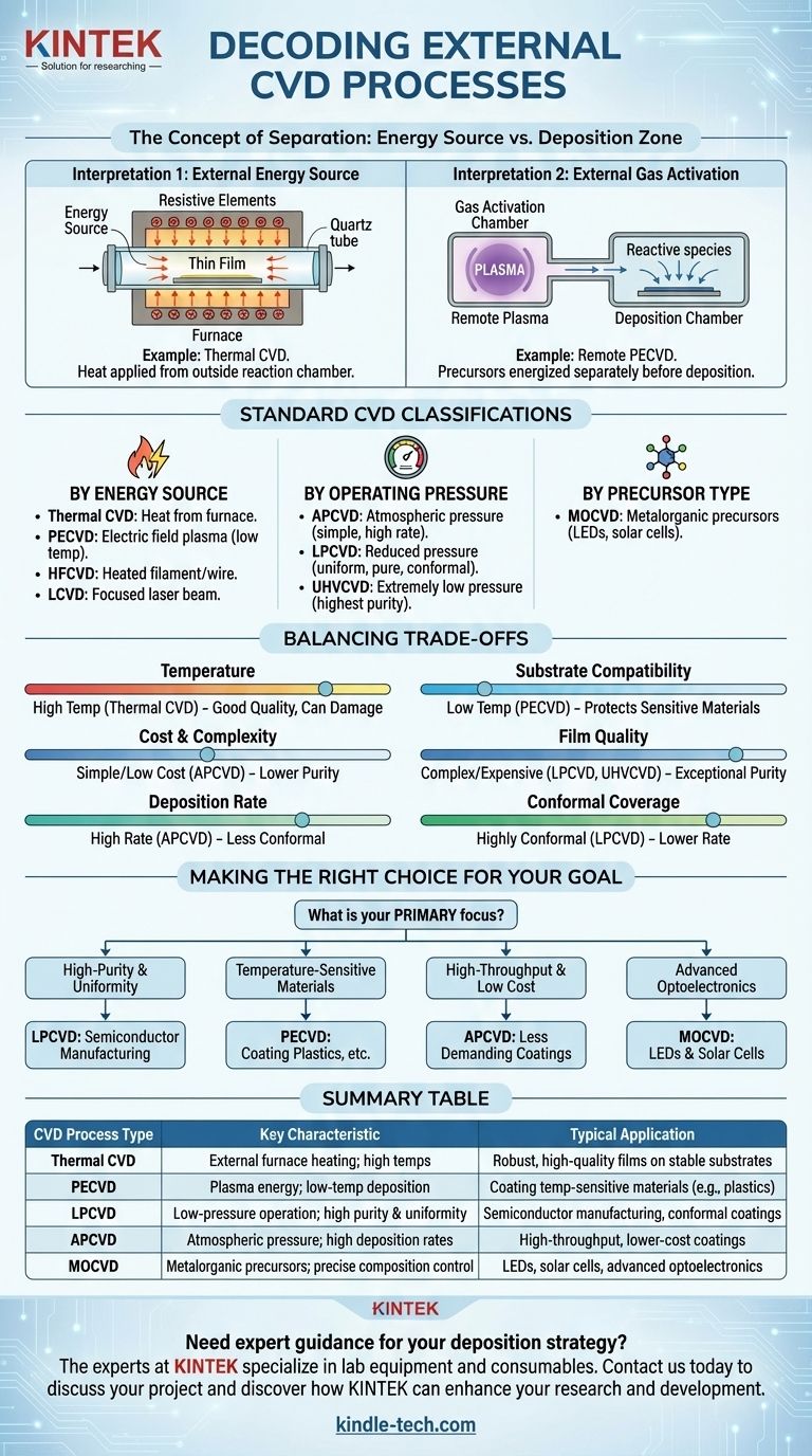
Interpretation 1: The Energy Source is External
In many common CVD systems, the energy required to drive the chemical reactions is applied from outside the main reaction chamber.
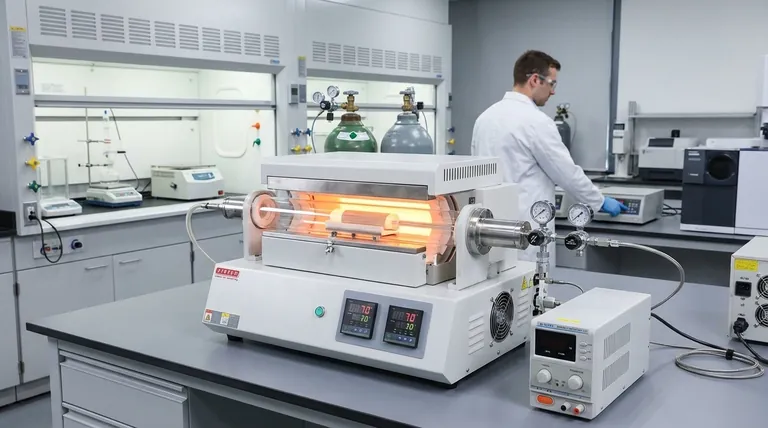
The most straightforward example is conventional Thermal CVD. Here, a furnace with resistive heating elements surrounds the quartz tube that serves as the reaction chamber. The energy is transferred through the chamber walls to heat the precursor gases and the substrate, initiating deposition. The heat source is clearly external to the reaction environment.
Interpretation 2: The Gas Activation is External
A more sophisticated interpretation involves processes where precursor gases are energized or decomposed into reactive species in a separate chamber before they are introduced to the main deposition chamber.
This is the principle behind Remote Plasma-Enhanced CVD (RPECVD). In this setup, a plasma is generated in an "external" chamber to break down precursor gases. These reactive, but electrically neutral, species then flow into the main chamber to deposit on the substrate. This prevents the substrate from being directly damaged by ion bombardment from the plasma itself.
The Standard Classifications of CVD Processes
To properly understand the landscape, it's crucial to use the industry-standard classifications. Engineers and scientists categorize CVD processes based on more precise operational parameters.
By Energy Source
The method used to provide energy for the chemical reaction is a primary differentiator.
- Thermal CVD: Uses heat from a furnace to decompose precursor gases. It is a robust and widely used method.
- Plasma-Enhanced CVD (PECVD): Uses an electric field to generate a plasma (an ionized gas). The high-energy electrons in the plasma break down precursor molecules, allowing deposition to occur at much lower temperatures than Thermal CVD.
- Hot-Filament CVD (HFCVD): Employs a heated wire or filament placed near the substrate to thermally decompose the precursor gases.
- Laser CVD (LCVD): Uses a focused laser beam to locally heat the substrate or the gas, allowing for precise, patterned deposition.
By Operating Pressure
The pressure inside the reaction chamber profoundly affects the quality and characteristics of the deposited film.
- Atmospheric Pressure CVD (APCVD): Operates at standard atmospheric pressure. It is simpler and allows for high deposition rates but can result in lower film purity and uniformity.
- Low-Pressure CVD (LPCVD): Operates at reduced pressures (typically 0.1-100 Pa). This slows down gas-phase reactions, leading to highly uniform and pure films that conform well to complex surface topographies.
- Ultra-High Vacuum CVD (UHVCVD): Operates under extremely low pressures to achieve the highest possible film purity, which is critical for advanced semiconductor applications.
By Precursor Type
Sometimes, the process is named after the specific chemical precursors used.
Metalorganic CVD (MOCVD) is a prominent example. This process uses metalorganic compounds—molecules containing both metal and carbon atoms—as precursors. It is a key technology for manufacturing high-performance LEDs and solar cells.
Understanding the Trade-offs
Choosing a CVD process always involves balancing competing factors. No single method is superior for all applications; the selection depends entirely on the desired outcome and constraints.
Temperature vs. Substrate Compatibility
High-temperature processes like Thermal CVD often produce high-quality, dense films. However, these high temperatures can damage or warp sensitive substrates, such as plastics or fully processed semiconductor wafers. PECVD is the solution here, as its use of plasma allows for high-quality deposition at much lower temperatures.
Cost and Complexity vs. Film Quality
APCVD systems are relatively simple and inexpensive to operate, making them suitable for high-volume, lower-cost applications. In contrast, LPCVD and UHVCVD systems are more complex and expensive due to their vacuum requirements but are necessary for the exceptional purity and uniformity demanded by the microelectronics industry.
Deposition Rate vs. Conformal Coverage
There is often a trade-off between the speed of deposition and the film's ability to uniformly coat complex, three-dimensional structures (its "conformality"). Processes like LPCVD excel at producing highly conformal films but may have lower deposition rates than APCVD.
Making the Right Choice for Your Goal
The optimal CVD method is dictated by the specific requirements of your material, substrate, and final application.
- If your primary focus is high-purity, uniform films on complex surfaces: LPCVD is often the superior choice for applications like semiconductor manufacturing.
- If your primary focus is deposition on temperature-sensitive materials: PECVD is the necessary technology to avoid damaging the underlying substrate.
- If your primary focus is high-throughput, low-cost coatings: APCVD provides a simple and fast method suitable for less demanding applications.
- If your primary focus is creating advanced optoelectronic devices: MOCVD is the industry-standard process due to its precise control over composition and crystal quality.
Ultimately, understanding the fundamental trade-offs between temperature, pressure, and energy source empowers you to select the most effective deposition strategy for your technical objective.
Summary Table:
| CVD Process Type | Key Characteristic | Typical Application |
|---|---|---|
| Thermal CVD | External furnace heating; high temperatures | Robust, high-quality films on stable substrates |
| PECVD | Plasma energy; low-temperature deposition | Coating temperature-sensitive materials (e.g., plastics) |
| LPCVD | Low-pressure operation; high purity & uniformity | Semiconductor manufacturing, conformal coatings |
| APCVD | Atmospheric pressure; high deposition rates | High-throughput, lower-cost coatings |
| MOCVD | Metalorganic precursors; precise composition control | LEDs, solar cells, advanced optoelectronics |
Need to select the right CVD process for your specific material and substrate? The experts at KINTEK are here to help. We specialize in lab equipment and consumables for all your laboratory needs. Our team can guide you to the optimal deposition strategy—whether you require high-purity LPCVD films, low-temperature PECVD coatings, or high-throughput APCVD solutions. Contact us today to discuss your project and discover how KINTEK can enhance your research and development.
Visual Guide
Related Products
- CVD Diamond Domes for Industrial and Scientific Applications
- Customer Made Versatile CVD Tube Furnace Chemical Vapor Deposition Chamber System Equipment
- Multi Heating Zones CVD Tube Furnace Machine Chemical Vapor Deposition Chamber System Equipment
- Chemical Vapor Deposition CVD Equipment System Chamber Slide PECVD Tube Furnace with Liquid Gasifier PECVD Machine
- CVD Diamond Optical Windows for Lab Applications
People Also Ask
- What is chemical vapor deposition of diamond? Grow High-Purity Diamonds Atom-by-Atom
- Are CVD diamonds real? Yes, and they are chemically identical to mined diamonds.
- How long does it take to make synthetic diamonds? Discover the 6-8 Week Science Behind Lab-Grown Gems
- What color diamonds are CVD? Understanding the Process from Brown Tint to Colorless Beauty
- Does the chemical vapor deposition be used for diamonds? Yes, for Growing High-Purity Lab Diamonds


