At its core, vapor phase deposition offers a powerful method for creating exceptionally pure, uniform, and high-performance thin films on a substrate. Its key advantages include remarkable versatility in materials, excellent coating adhesion, and the ability to produce highly controlled layers, making it a cornerstone technology in industries from electronics to aerospace.
Vapor phase deposition should not be viewed as a single technique, but as a family of processes. Its fundamental advantage lies in the atomic-level control it provides, enabling the engineering of materials and coatings with properties that are often impossible to achieve through conventional means.
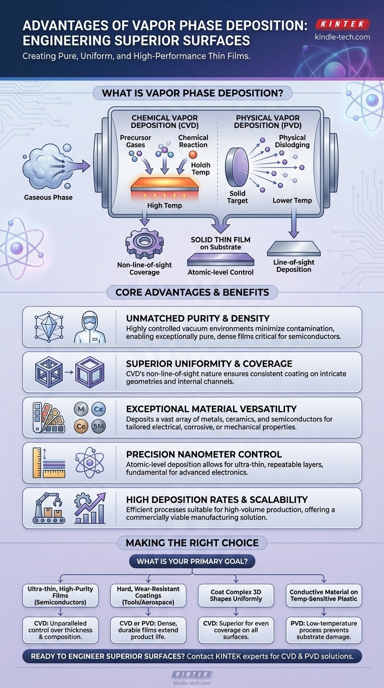
What is Vapor Phase Deposition?
Vapor phase deposition is a general term for processes where a material is converted into a gaseous phase, transported, and then condensed as a solid film onto a surface (the substrate). This atom-by-atom or molecule-by-molecule buildup is what allows for such precision.
The two main families of this technology are Chemical Vapor Deposition (CVD) and Physical Vapor Deposition (PVD). While they share the goal of creating a thin film, the way they achieve it differs significantly and impacts their specific advantages.
The Core Advantages of Vapor Deposition
While specific benefits vary by method, the entire class of vapor deposition techniques is valued for several shared characteristics.
Unmatched Purity and Density
Vapor deposition processes occur in highly controlled environments, often under vacuum. This minimizes contamination and allows for the creation of exceptionally pure and dense films or nanoparticles.
This high purity is critical for applications like semiconductors, where even tiny impurities can ruin a device's performance.
Superior Uniformity and Coverage
A major advantage, particularly for CVD, is its non-line-of-sight nature. The precursor gases flow around an object, reacting on all exposed surfaces.
This allows for a completely uniform coating on components with complex shapes, internal channels, or intricate geometries that would be impossible to coat evenly with line-of-sight techniques like spraying.
Exceptional Versatility of Materials
Vapor deposition is not limited to a single type of material. It can be used to deposit a vast array of metallic, ceramic, and semiconducting films.
This versatility allows engineers to select the perfect coating material for a specific performance goal, whether it's electrical conductivity, corrosion resistance, or hardness.
Precision Control Down to the Nanometer
Because material is deposited on an atomic scale, these processes offer incredible control over the final product. It's possible to create ultra-thin layers of material with precise, repeatable thickness.
This level of control is fundamental to the manufacturing of modern electrical circuits and optical films, where layer thickness directly dictates performance.
High Deposition Rates and Scalability
Compared to other atomic-level techniques, many vapor deposition processes offer relatively high deposition rates and excellent manufacturing yields.
Once a process is established, it is often straightforward to scale up for high-volume production, making it a commercially viable solution.
Understanding the Trade-offs and Key Differences
To truly leverage this technology, you must understand the distinction between its two primary forms and their inherent trade-offs.
Chemical vs. Physical Deposition
Chemical Vapor Deposition (CVD) involves introducing precursor gases into a chamber, which then chemically react on the hot substrate's surface to form the desired film.
Physical Vapor Deposition (PVD) does not use chemical reactions. Instead, it physically dislodges material from a solid source (the "target") via methods like sputtering or vaporization with an arc. This vaporized material then travels and condenses on the substrate.
Substrate and Temperature Sensitivity
A key trade-off for CVD is its reliance on high temperatures to drive the necessary chemical reactions. This can limit the types of substrates that can be used, as some materials cannot withstand the heat.
Conversely, some PVD methods, like cathodic arc deposition, generate very little radiant heat, making them suitable for more temperature-sensitive substrates.
Line-of-Sight Limitations
The non-line-of-sight capability of CVD is one of its defining strengths. However, most PVD processes are line-of-sight.
This means PVD is excellent for coating flat surfaces or simple shapes but struggles to coat the inside of tubes or complex, shadowed geometries without sophisticated part manipulation.
Making the Right Choice for Your Application
Selecting the right vapor deposition method requires aligning its specific strengths with your primary engineering goal.
- If your primary focus is producing ultra-thin, high-purity films for semiconductors: CVD offers unparalleled control over layer thickness and composition for building complex electronic structures.
- If your primary focus is applying hard, wear-resistant coatings to tools or aerospace components: Both PVD and CVD are excellent choices, offering dense, durable films that dramatically extend product life and performance.
- If your primary focus is coating complex 3D shapes uniformly: CVD is often the superior method due to its inherent non-line-of-sight nature, ensuring even coverage on all surfaces.
- If your primary focus is depositing a conductive material onto a temperature-sensitive plastic: A low-temperature PVD process would be a more suitable choice than a traditional high-temperature CVD process.
Ultimately, understanding these processes empowers you to engineer surfaces and materials for peak performance in their intended environment.
Summary Table:
| Advantage | Description | Key Benefit |
|---|---|---|
| Unmatched Purity & Density | Highly controlled vacuum environments minimize contamination. | Critical for semiconductor performance and reliability. |
| Superior Uniformity & Coverage | Non-line-of-sight (CVD) coating for complex 3D shapes. | Ensures consistent coating on intricate geometries and internal channels. |
| Exceptional Material Versatility | Deposits a wide range of metals, ceramics, and semiconductors. | Enables tailored coatings for specific electrical, corrosive, or mechanical needs. |
| Precision Nanometer Control | Atomic-level deposition for ultra-thin, repeatable layers. | Fundamental for manufacturing advanced electronics and optical films. |
| High Deposition Rates & Scalability | Efficient processes suitable for high-volume production. | Offers a commercially viable solution for industrial manufacturing. |
Ready to Engineer Superior Surfaces with Vapor Phase Deposition?
Whether you are developing next-generation semiconductors, applying wear-resistant coatings to aerospace components, or need to uniformly coat complex 3D parts, choosing the right deposition method is critical. KINTEK specializes in providing advanced lab equipment and consumables for both Chemical Vapor Deposition (CVD) and Physical Vapor Deposition (PVD) processes.
We can help you select the ideal solution to achieve the high purity, uniformity, and precision your laboratory demands. Contact our experts today to discuss how our vapor phase deposition solutions can enhance your research and production outcomes.
Visual Guide
Related Products
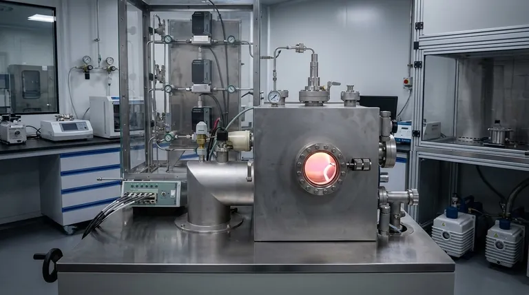
- Microwave Plasma Chemical Vapor Deposition MPCVD Machine System Reactor for Lab and Diamond Growth
- RF PECVD System Radio Frequency Plasma-Enhanced Chemical Vapor Deposition RF PECVD
- Chemical Vapor Deposition CVD Equipment System Chamber Slide PECVD Tube Furnace with Liquid Gasifier PECVD Machine
- 915MHz MPCVD Diamond Machine Microwave Plasma Chemical Vapor Deposition System Reactor
- Inclined Rotary Plasma Enhanced Chemical Vapor Deposition PECVD Equipment Tube Furnace Machine
People Also Ask
- What are the advantages of a Microwave Plasma CVD reactor for MCD/NCD coatings? Precision Multilayer Diamond Engineering
- What is microwave plasma chemical vapor deposition? A Guide to High-Purity Diamond Film Growth
- How does a microwave plasma reactor facilitate the synthesis of diamond? Master MPCVD with Precision Technology
- Why is argon-rich gas phase chemistry used for UNCD growth? Unlock Precision Nano-Diamond Synthesis
- How do vacuum pumps and valves collaborate in MPCVD? Achieve Precise Pressure Control for Superior CNT Synthesis


