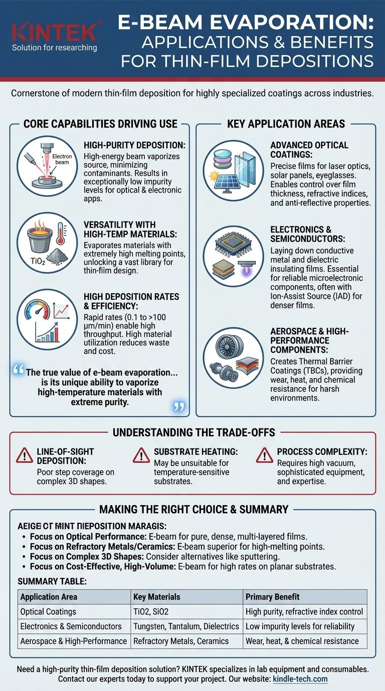
Electron beam evaporation is a cornerstone of modern thin-film deposition, used to create highly specialized coatings across industries like optics, electronics, and aerospace. Its primary applications involve depositing exceptionally pure, dense films of materials—including those with very high melting points—to achieve specific optical properties or provide resistance to heat, wear, and chemicals.
The true value of e-beam evaporation isn't just its wide range of applications, but its unique ability to vaporize high-temperature materials with extreme purity. This makes it the definitive choice for creating advanced optical coatings and high-performance electronic components where material integrity cannot be compromised.
The Core Capabilities Driving Its Use
To understand where e-beam evaporation is applied, you must first understand its fundamental advantages over other deposition methods.
High-Purity Deposition
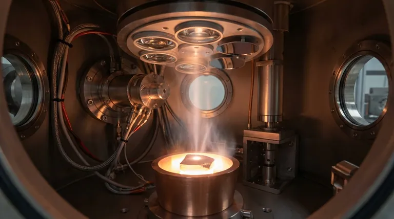
The process works by firing a high-energy beam of electrons at a source material (or "puck") inside a high-vacuum chamber. This directly heats only the source material, causing it to evaporate.
Because no crucible or filament heats the material indirectly, the risk of introducing contaminants into the vapor stream is minimized. This results in films with exceptionally low impurity levels, a critical requirement for many optical and electronic applications.
Versatility with High-Temperature Materials
Many advanced materials, such as refractory metals (e.g., tungsten, tantalum) and ceramics (e.g., titanium dioxide, silicon dioxide), have extremely high melting points.
E-beam evaporation can generate enough focused energy to vaporize these materials, a task that is difficult or impossible for other methods like standard thermal evaporation. This unlocks a vast library of materials for thin-film design.
High Deposition Rates and Efficiency
E-beam evaporation is known for its rapid deposition rates, ranging from 0.1 to over 100 micrometers per minute. This enables high throughput for manufacturing.
Furthermore, because the beam can be precisely focused on the source material, it offers high material utilization efficiency, reducing waste and lowering costs compared to processes like sputtering.
Key Application Areas
These core capabilities make e-beam evaporation the ideal solution for several key markets.
Advanced Optical Coatings
This is the most prominent application. E-beam is used to deposit precise, multi-layered films for laser optics, solar panels, prescription eyeglasses, and architectural glass.
The process allows for meticulous control over film thickness and density, which is essential for achieving specific refractive indices, anti-reflective properties, and high laser damage thresholds.
Electronics and Semiconductors
In electronics, e-beam evaporation is used to lay down conductive metal layers and dielectric insulating films. Its ability to create high-purity films is critical for ensuring reliable performance in microelectronic components.
The process can also be combined with an ion-assist source (IAD), which bombards the substrate with ions during deposition to create even denser, more durable films with better adhesion.
Aerospace and High-Performance Components
The aerospace, automotive, and energy industries use e-beam evaporation to create thermal barrier coatings (TBCs) and layers that provide wear and chemical resistance.
The technology’s ability to deposit durable, dense films of high-temperature ceramics makes it perfect for protecting components that operate in harsh environments, such as turbine blades.
Understanding the Trade-offs
No technology is a universal solution. The strengths of e-beam evaporation also define its limitations.
Line-of-Sight Deposition
E-beam evaporation is a line-of-sight process, meaning the evaporated material travels in a straight line from the source to the substrate.
While this directionality is beneficial for some applications, it results in poor "step coverage" on substrates with complex, three-dimensional topographies. Features not directly in the path of the vapor stream will receive little or no coating. Planetary rotation systems are often required to mitigate this and improve uniformity.
Substrate Heating
The significant energy required to vaporize the source material radiates throughout the chamber, which can heat the substrate. This may be unsuitable for depositing films onto temperature-sensitive substrates, such as certain plastics or biological components.
Process Complexity
Maintaining a high-vacuum environment and precisely controlling the electron beam requires sophisticated and expensive equipment. The process demands significant expertise to manage deposition rates and ensure film uniformity, making it more complex than some alternative methods.
Making the Right Choice for Your Project
Selecting a deposition method depends entirely on your project's primary goal.
- If your primary focus is optical performance: E-beam is the industry standard for creating the pure, dense, and multi-layered films required for precision optics.
- If your primary focus is depositing refractory metals or ceramics: E-beam's ability to handle high-melting-point materials makes it a superior choice over thermal evaporation.
- If your primary focus is coating complex 3D shapes uniformly: You must carefully evaluate e-beam's line-of-sight limitations and consider alternatives like sputtering for superior step coverage.
- If your primary focus is cost-effective, high-volume production: E-beam's high deposition rates and material efficiency make it highly competitive, especially for planar substrates.
Understanding these core capabilities allows you to select e-beam evaporation with confidence for applications where purity and material integrity are non-negotiable.
Summary Table:
| Application Area | Key Materials Used | Primary Benefit |
|---|---|---|
| Optical Coatings | Titanium Dioxide, Silicon Dioxide | High purity, precise refractive index control |
| Electronics & Semiconductors | Tungsten, Tantalum, Dielectrics | Low impurity levels for reliable performance |
| Aerospace & High-Performance | Refractory Metals, Ceramics | Wear, heat, and chemical resistance |
Need a high-purity thin-film deposition solution for your lab?
KINTEK specializes in lab equipment and consumables, serving laboratory needs. Our expertise in e-beam evaporation systems can help you achieve the material integrity and performance required for your most demanding optical, electronic, or high-temperature coating applications.
Contact our experts today to discuss how we can support your project with the right equipment and solutions.
Visual Guide
Related Products
- Electron Beam Evaporation Coating Oxygen-Free Copper Crucible and Evaporation Boat
- Electron Beam Evaporation Coating Tungsten Crucible and Molybdenum Crucible for High Temperature Applications
- Electron Beam Evaporation Coating Gold Plating Tungsten Molybdenum Crucible for Evaporation
- Electron Beam Evaporation Coating Conductive Boron Nitride Crucible BN Crucible
- E Beam Crucibles Electron Gun Beam Crucible for Evaporation
People Also Ask
- What is the container that holds the metal source material called in e-beam evaporation? Ensure Purity and Quality in Your Thin-Film Deposition
- What is the current of e-beam evaporation? A Guide to High-Purity Thin Film Deposition
- What is the temperature of e-beam evaporation? Mastering the Two-Zone Thermal Process for Precision Films
- What is the deposition rate of e-beam evaporation? Control Thin Film Quality and Speed
- What is e-beam evaporation? Achieve High-Purity Thin Film Deposition for Your Lab


