In short, thin films are ultra-thin layers of material, ranging from fractions of a nanometer to several micrometers thick, that are deposited onto a surface to grant it new or enhanced properties. Their applications span nearly every modern industry, including electronics (for integrated circuits and transistors), optics (for anti-reflective coatings), energy (for solar cells and batteries), and manufacturing (for protective hard coatings on tools).
The true power of thin films lies not in the material itself, but in their ability to fundamentally change the function of a surface. By applying an engineered layer, we can make glass reflective, metal conductive, or a medical implant biocompatible, turning simple substrates into high-performance components.
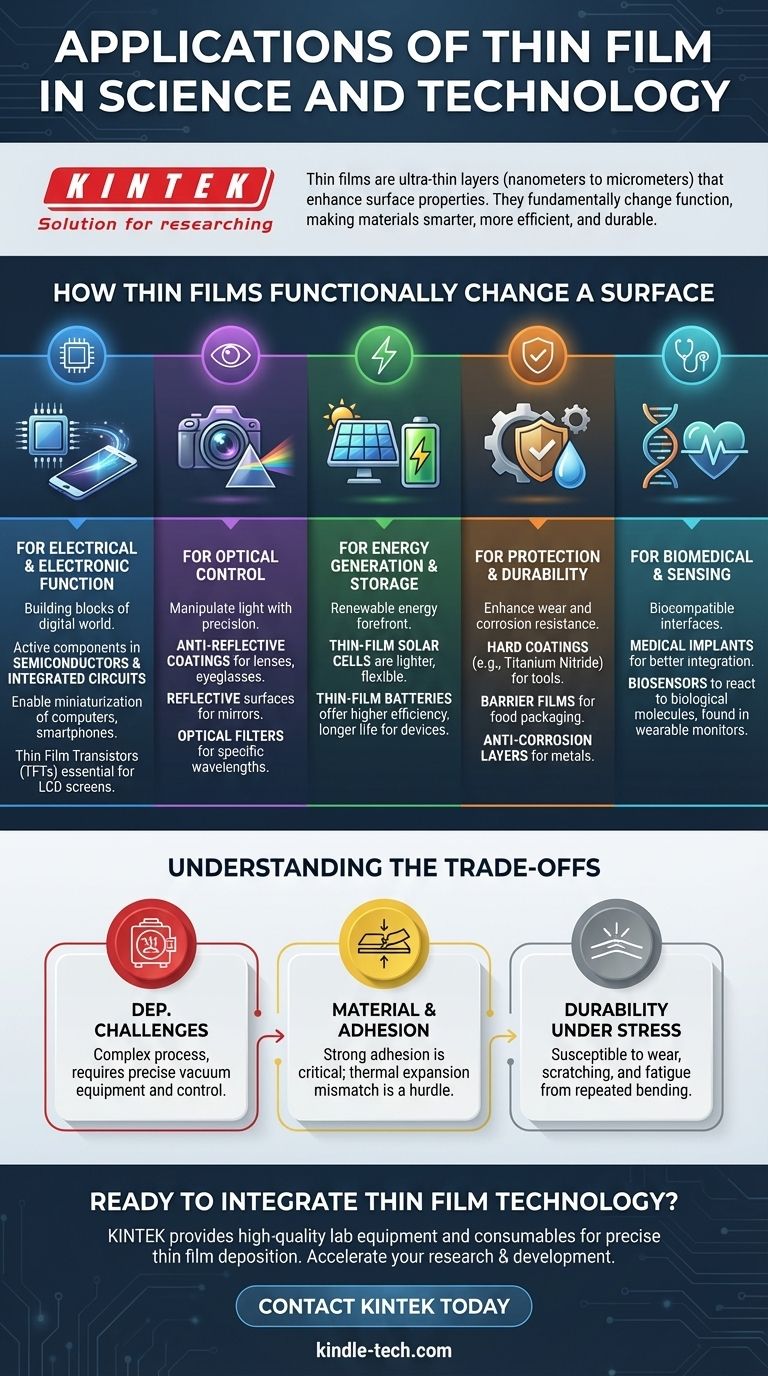
How Thin Films Functionally Change a Surface
The versatility of thin film technology comes from its ability to impart specific electrical, optical, or physical properties to a base material, known as a substrate. This is typically done by categorizing the application based on its primary function.
For Electrical and Electronic Function
The entire digital world is built upon thin films. They are the active components in semiconductors and integrated circuits.
By depositing precise layers of different materials, we create the microscopic transistors and pathways that allow processors and memory chips to function. This is what enables the miniaturization and power of computers, smartphones, and countless other devices.
Thin film transistors (TFTs) are also essential for modern screens, such as liquid crystal displays (LCDs), where they act as tiny switches controlling each pixel, offering faster response times and greater energy efficiency.
For Optical Control
Thin films are used to manipulate light with incredible precision. You interact with these applications daily.
The anti-reflective coatings on your eyeglasses or a camera lens are thin films designed to minimize glare and maximize light transmission. The reflective surface of a household mirror is a simple thin film of metal.
More advanced applications include complex multi-layer coatings that create optical filters, which only allow specific colors or wavelengths of light to pass through. These are critical for scientific instruments, telecommunications, and automotive head-up displays.
For Energy Generation and Storage
Thin film technology is at the forefront of renewable energy. Thin-film solar cells are made by depositing photovoltaic material onto a substrate like glass or flexible plastic.
This makes solar panels lighter, more flexible, and suitable for applications like photovoltaic glazing on buildings. Similarly, thin-film batteries offer higher efficiency, faster charging, and longer lifespans, improving everything from medical implants and smart cards to large-scale energy storage banks.
For Protection and Durability
One of the most common industrial applications is adding a protective layer to a surface. Hard coatings of materials like titanium nitride are applied to cutting tools and machine parts to dramatically increase their wear resistance.
Thin polymer films are used in food packaging to create a barrier against oxygen and moisture, preserving freshness. Other films are designed specifically to prevent corrosion on metals, extending the life of components in aerospace, automotive, and marine environments.
For Biomedical and Sensing Applications
In medicine, thin films must be biocompatible, meaning they don't harm living tissue. They are used to coat medical implants to improve their integration with the body and prevent rejection.
They are also the key component in many biosensors, where a specific film is designed to react to the presence of a particular biological molecule. This technology is found in wearable health monitors, diagnostic tools, and hearing aids.
Understanding the Trade-offs
While incredibly powerful, thin film technology is not without its challenges. The primary trade-offs revolve around the complexity of production and the inherent delicacy of the films themselves.
The Challenge of Deposition
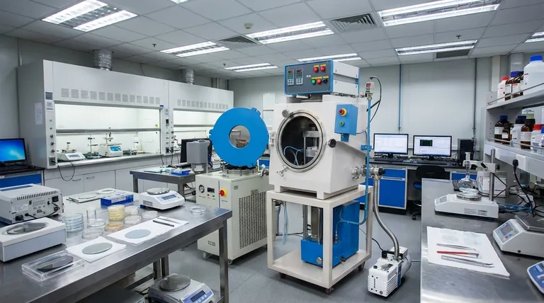
Creating a perfectly uniform film that is only a few atoms thick is a highly sophisticated process. It requires specialized, expensive vacuum equipment and precise control over temperature, pressure, and source materials. Any impurity or variation can ruin the film's desired properties.
Material Constraints and Adhesion
Not every material can be easily deposited as a thin film. Furthermore, ensuring the film adheres strongly to the underlying substrate without peeling or cracking is a major engineering challenge, especially when the two materials have different thermal expansion rates.
Durability Under Stress
By definition, a thin film is not a bulk material. While protective coatings are very hard, they can be scratched or worn away, exposing the substrate underneath. Flexible electronic devices depend on films that can withstand repeated bending without failure, which remains a key area of research.
Matching the Film to the Function
To apply this technology effectively, you must align the type of thin film and deposition process with your specific goal.
- If your primary focus is advancing electronics: Concentrate on semiconductor materials and complex layering techniques to create smaller, faster, and more efficient microelectronic devices and displays.
- If your primary focus is improving energy systems: Investigate photovoltaic materials for solar cells and solid-state electrolytes for thin-film batteries to boost efficiency and create new, flexible form factors.
- If your primary focus is enhancing material properties: Explore hard, optical, and decorative coatings that can add immense value to common substrates by making them more durable, functional, or aesthetically pleasing.
- If your primary focus is developing medical technology: Focus on biocompatible and functionalized films that can serve as the interface between technology and biology in sensors, implants, and smart pharmaceutical delivery.
Ultimately, thin film technology is the invisible layer that underpins much of modern science and engineering, enabling us to create materials that perform far beyond their natural limits.
Summary Table:
| Application Area | Key Functions & Examples |
|---|---|
| Electronics & Semiconductors | Integrated circuits, transistors, TFTs for LCD displays. |
| Optics | Anti-reflective coatings, mirrors, optical filters. |
| Energy | Thin-film solar cells, high-efficiency batteries. |
| Protective Coatings | Hard coatings for tools, anti-corrosion layers. |
| Biomedical | Biocompatible implants, biosensors for health monitoring. |
Ready to Integrate Thin Film Technology into Your Projects?
Thin film deposition is a precise science, and the right equipment is crucial for success. Whether you are developing advanced semiconductors, high-efficiency solar cells, durable protective coatings, or sensitive biomedical sensors, KINTEK provides the high-quality lab equipment and consumables you need.
We specialize in supporting laboratory innovation with reliable deposition systems and expert support. Let us help you achieve the perfect film for your application.
Contact KINTEL today to discuss your specific requirements and discover how our solutions can accelerate your research and development.
Visual Guide
Related Products
- Aluminized Ceramic Evaporation Boat for Thin Film Deposition
- Tungsten Evaporation Boat for Thin Film Deposition
- Electron Beam Evaporation Coating Oxygen-Free Copper Crucible and Evaporation Boat
- Molybdenum Tungsten Tantalum Evaporation Boat for High Temperature Applications
- Aluminum-Plastic Flexible Packaging Film for Lithium Battery Packaging
People Also Ask
- Why is an alumina boat and Ti3AlC2 powder bed necessary for Ti2AlC sintering? Protect MAX Phase Purity
- What are the applications of thin films deposition? Unlock New Possibilities for Your Materials
- What is the widely used boat made of in thermal evaporation? Choosing the Right Material for High-Purity Deposition
- What are the alternatives to sputtering? Choose the Right Thin Film Deposition Method
- What is the source of evaporation for thin film? Choosing Between Thermal and E-Beam Methods


