Knowledge What are thin film materials used for? Powering Electronics, Optics, and Medical Devices
Author avatar

Tech Team · Kintek Solution

Updated 5 days ago

What are thin film materials used for? Powering Electronics, Optics, and Medical Devices


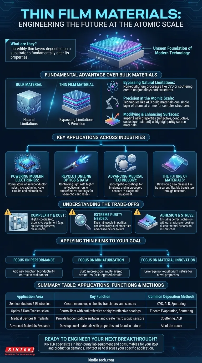
At their core, thin film materials are incredibly thin layers of specific substances deposited onto a surface, or substrate, to fundamentally alter its properties. These materials are the unseen foundation of modern technology, used in everything from semiconductor manufacturing and fiberoptic systems to advanced medical devices and consumer electronics.

The true power of thin films lies in their unique manufacturing process, which allows for the creation of material structures and properties that are often impossible to achieve in a material's normal, or "bulk," state. This enables the precise engineering of surfaces for specific electronic, optical, or physical functions.

What are thin film materials used for? Powering Electronics, Optics, and Medical Devices

The Fundamental Advantage Over Bulk Materials

To understand the widespread use of thin films, you must first understand why they are fundamentally different from standard materials. The key is in how they are made.

Bypassing Natural Limitations

Most methods for creating thin films, such as Chemical Vapor Deposition (CVD) or sputtering, are "non-equilibrium" processes.

This means the material is deposited atom by atom in a way that is not constrained by the rules of standard metallurgy. It allows engineers to create unique alloys and structures that wouldn't form naturally.

Precision at the Atomic Scale

Techniques like Atomic Layer Deposition (ALD) give manufacturers an extraordinary level of control, allowing them to build a material one single layer of atoms at a time.

This precision is essential for creating the incredibly complex, layered structures required for modern microchips and sensors.

Modifying and Enhancing Surfaces

The primary goal of a thin film is to impart a new property to the surface of a substrate. A film can make a material reflective, electrically conductive, resistant to corrosion, or harder than it was before.

These films are formed using high-purity source materials, such as precursor gases or solid sputtering targets, to ensure the final layer has the exact properties required.

Key Applications Across Industries

The ability to precisely control surface properties has made thin films indispensable in nearly every high-tech field.

Powering Modern Electronics

Thin film deposition is the cornerstone of the semiconductor industry. The intricate circuits inside a computer processor are built by depositing dozens of different thin films of conductive, insulating, and semiconducting materials.

Revolutionizing Optics and Data

In fiberoptic systems and industrial lasers, thin films are used to create highly reflective mirrors or anti-reflective coatings. These coatings precisely control how light behaves, which is critical for data transmission and imaging.

Advancing Medical Technology

Thin films are essential in biomedical devices and medical electronics. They can create biocompatible coatings for implants or form the microscopic electrodes and sensors used in advanced diagnostic equipment.

The Future of Materials

Research is constantly pushing the boundaries of what is possible. New classes of thin films, such as amorphous heavy-metal cation multicomponent oxides, are being developed to create technologies like transparent, flexible transistors.

Understanding the Trade-offs

While powerful, working with thin film materials involves significant technical challenges that are important to recognize.

Complexity and Cost of Deposition

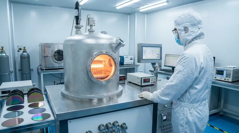
The equipment required for thin film deposition, such as electron beam evaporators or magnetron sputtering systems, is highly specialized and expensive. It requires operation in controlled environments, like cleanrooms, adding to the complexity.

The Need for Extreme Purity

The performance of a thin film is directly tied to the purity of its source materials. Even minuscule impurities can drastically alter the film's electrical or optical properties, leading to device failure.

Adhesion and Stress

Ensuring a microscopic film adheres perfectly to its substrate without cracking or peeling is a major engineering challenge. Mismatches in thermal expansion or internal stress can ruin the integrity of the entire component.

Applying Thin Films to Your Goal

Your reason for using a thin film will determine which properties and processes are most important.

  • If your primary focus is performance: Use thin films to add a new function—like anti-reflection, conductivity, or corrosion resistance—to an existing substrate.
  • If your primary focus is miniaturization: Thin film deposition is the only viable method for building the microscopic, multi-layered structures at the heart of integrated circuits and sensors.
  • If your primary focus is material innovation: Leverage the non-equilibrium nature of deposition to create novel material compositions with properties that cannot be found in nature.

Ultimately, thin films empower us to engineer the behavior of matter at its most fundamental level.

Summary Table:

Application Area Key Function of Thin Films Common Deposition Methods
Semiconductors & Electronics Create microscopic circuits, transistors, and sensors CVD, ALD, Sputtering
Optics & Data Transmission Control light with anti-reflective or highly reflective coatings E-beam Evaporation, Sputtering
Medical Devices & Implants Provide biocompatible surfaces and create microscopic sensors Sputtering, ALD
Advanced Materials Research Develop novel materials with properties not found in nature All of the above

Ready to Engineer Your Next Breakthrough with Thin Films?

Thin film deposition is the key to creating the next generation of high-performance devices. KINTEK specializes in providing the high-purity lab equipment and consumables—from sputtering targets to precision deposition systems—that your R&D or production process demands.

Whether you're developing advanced semiconductors, optical coatings, or biomedical sensors, we have the expertise and products to support your goals.

Contact KINTEK today to discuss your specific application and discover how our solutions can enhance your thin film projects.

Visual Guide

What are thin film materials used for? Powering Electronics, Optics, and Medical Devices Visual Guide

Related Products

People Also Ask

Related Products

HFCVD Machine System Equipment for Drawing Die Nano-Diamond Coating

HFCVD Machine System Equipment for Drawing Die Nano-Diamond Coating

The nano-diamond composite coating drawing die uses cemented carbide (WC-Co) as the substrate, and uses the chemical vapor phase method ( CVD method for short ) to coat the conventional diamond and nano-diamond composite coating on the surface of the inner hole of the mold.

Vacuum Hot Press Furnace Machine for Lamination and Heating

Vacuum Hot Press Furnace Machine for Lamination and Heating

Experience clean and precise lamination with Vacuum Lamination Press. Perfect for wafer bonding, thin-film transformations, and LCP lamination. Order now!

915MHz MPCVD Diamond Machine Microwave Plasma Chemical Vapor Deposition System Reactor

915MHz MPCVD Diamond Machine Microwave Plasma Chemical Vapor Deposition System Reactor

915MHz MPCVD Diamond Machine and its multi-crystal effective growth, the maximum area can reach 8 inches, the maximum effective growth area of single crystal can reach 5 inches. This equipment is mainly used for the production of large-size polycrystalline diamond films, the growth of long single crystal diamonds, the low-temperature growth of high-quality graphene, and other materials that require energy provided by microwave plasma for growth.

CVD Diamond Cutting Tool Blanks for Precision Machining

CVD Diamond Cutting Tool Blanks for Precision Machining

CVD Diamond Cutting Tools: Superior Wear Resistance, Low Friction, High Thermal Conductivity for Non-Ferrous Materials, Ceramics, Composites Machining

Small Vacuum Heat Treat and Tungsten Wire Sintering Furnace

Small Vacuum Heat Treat and Tungsten Wire Sintering Furnace

The small vacuum tungsten wire sintering furnace is a compact experimental vacuum furnace specially designed for universities and scientific research institutes. The furnace features a CNC welded shell and vacuum piping to ensure leak-free operation. Quick-connect electrical connections facilitate relocation and debugging, and the standard electrical control cabinet is safe and convenient to operate.

Vacuum Dental Porcelain Sintering Furnace

Vacuum Dental Porcelain Sintering Furnace

Get precise and reliable results with KinTek's Vacuum Porcelain Furnace. Suitable for all porcelain powders, it features hyperbolic ceramic furnace function, voice prompt, and automatic temperature calibration.

Ultra-High Temperature Graphite Vacuum Graphitization Furnace

Ultra-High Temperature Graphite Vacuum Graphitization Furnace

The ultra-high temperature graphitization furnace utilizes medium frequency induction heating in a vacuum or inert gas environment. The induction coil generates an alternating magnetic field, inducing eddy currents in the graphite crucible, which heats up and radiates heat to the workpiece, bringing it to the desired temperature. This furnace is primarily used for graphitization and sintering of carbon materials, carbon fiber materials, and other composite materials.

1200℃ Split Tube Furnace with Quartz Tube Laboratory Tubular Furnace

1200℃ Split Tube Furnace with Quartz Tube Laboratory Tubular Furnace

KT-TF12 split tube furnace: high-purity insulation, embedded heating wire coils, and max. 1200C. Widely used for new materials and chemical vapour deposition.

Vacuum Heat Treat and Molybdenum Wire Sintering Furnace for Vacuum Sintering

Vacuum Heat Treat and Molybdenum Wire Sintering Furnace for Vacuum Sintering

A vacuum molybdenum wire sintering furnace is a vertical or bedroom structure, which is suitable for withdrawal, brazing, sintering and degassing of metal materials under high vacuum and high temperature conditions. It is also suitable for dehydroxylation treatment of quartz materials.

Graphite Vacuum Furnace High Thermal Conductivity Film Graphitization Furnace

Graphite Vacuum Furnace High Thermal Conductivity Film Graphitization Furnace

The high thermal conductivity film graphitization furnace has uniform temperature, low energy consumption and can operate continuously.

Graphite Vacuum Furnace IGBT Experimental Graphitization Furnace

Graphite Vacuum Furnace IGBT Experimental Graphitization Furnace

IGBT experimental graphitization furnace, a tailored solution for universities and research institutions, with high heating efficiency, user-friendliness, and precise temperature control.

Vacuum Sealed Continuous Working Rotary Tube Furnace Rotating Tube Furnace

Vacuum Sealed Continuous Working Rotary Tube Furnace Rotating Tube Furnace

Experience efficient material processing with our vacuum-sealed rotary tube furnace. Perfect for experiments or industrial production, equipped with optional features for controlled feeding and optimized results. Order now.

Laboratory Sterilizer Lab Autoclave Pulse Vacuum Lifting Sterilizer

Laboratory Sterilizer Lab Autoclave Pulse Vacuum Lifting Sterilizer

The pulse vacuum lifting sterilizer is a state-of-the-art equipment for efficient and precise sterilization. It uses pulsating vacuum technology, customizable cycles, and a user-friendly design for easy operation and safety.

Custom Machined and Molded PTFE Teflon Parts Manufacturer for Laboratory ITO FTO Conductive Glass Cleaning Flower Basket

Custom Machined and Molded PTFE Teflon Parts Manufacturer for Laboratory ITO FTO Conductive Glass Cleaning Flower Basket

PTFE cleaning racks are mainly made of tetrafluoroethylene. PTFE, known as the "King of Plastics", is a polymer compound made of tetrafluoroethylene.

Custom PTFE Teflon Parts Manufacturer for Gaskets and More

Custom PTFE Teflon Parts Manufacturer for Gaskets and More

Gaskets are materials placed between two flat surfaces to enhance the seal. To prevent fluid leakage, sealing elements are arranged between static sealing surfaces.

1700℃ Laboratory Quartz Tube Furnace with Alumina Tube Tubular Furnace

1700℃ Laboratory Quartz Tube Furnace with Alumina Tube Tubular Furnace

Looking for a high-temperature tube furnace? Check out our 1700℃ Tube Furnace with Alumina Tube. Perfect for research and industrial applications up to 1700C.

Benchtop Laboratory Vacuum Freeze Dryer

Benchtop Laboratory Vacuum Freeze Dryer

Benchtop laboratory freeze dryer for efficient lyophilization of biological, pharmaceutical, and food samples. Features intuitive touchscreen, high-performance refrigeration, and durable design. Preserve sample integrity—consult now!

Laboratory Sterilizer Lab Autoclave Vertical Pressure Steam Sterilizer for Liquid Crystal Display Automatic Type

Laboratory Sterilizer Lab Autoclave Vertical Pressure Steam Sterilizer for Liquid Crystal Display Automatic Type

Liquid crystal display automatic vertical sterilizer is a safe, reliable and automatic control sterilization equipment, which is composed of heating system, microcomputer control system and overheating and overvoltage protection system.

Anti-Cracking Press Mold for Lab Use

Anti-Cracking Press Mold for Lab Use

The anti-cracking press mold is a specialized equipment designed for molding various shapes and sizes of film using high pressure and electric heating.

Benchtop Laboratory Freeze Dryer for Lab Use

Benchtop Laboratory Freeze Dryer for Lab Use

Premium benchtop laboratory freeze dryer for lyophilization, preserving samples with ≤ -60°C cooling. Ideal for pharmaceuticals & research.


Leave Your Message