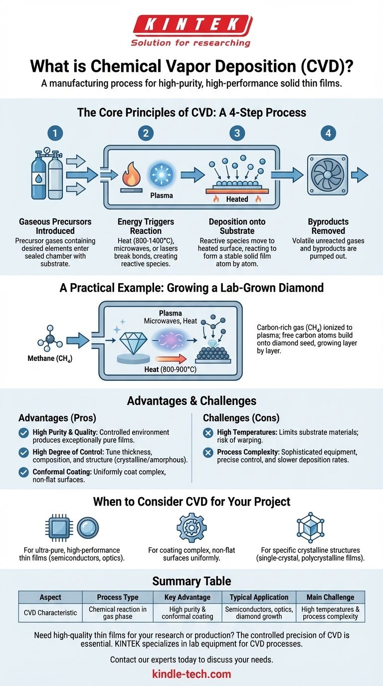
In essence, Chemical Vapor Deposition (CVD) is a manufacturing process used to create high-purity, high-performance solid thin films on a surface. It works by introducing one or more gaseous chemical precursors into a reaction chamber, which then react or decompose near a heated substrate, causing a thin layer of the desired material to deposit onto it.
The core principle of CVD is using controlled chemical reactions in a gas phase to build a solid material layer by layer. This chemical nature distinguishes it from physical processes and gives engineers precise control over the final film's purity, structure, and properties.
The Core Principles of CVD
To understand CVD, it's best to break it down into its fundamental steps. The process is a carefully orchestrated sequence of events occurring within a controlled reaction chamber.
Step 1: Gaseous Precursors are Introduced
The entire process begins with gases. These "precursor" gases contain the elements required for the final film and are pumped into a sealed chamber containing the object to be coated, known as the substrate.
Step 2: Energy Triggers a Chemical Reaction
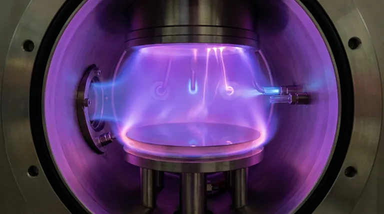
High energy is applied to the chamber, typically in the form of heat. Temperatures often range from 800°C to over 1400°C, activated by methods like microwaves, lasers, or a hot filament.
This energy breaks the chemical bonds within the precursor gases, making them highly reactive. This is the central "chemical" event in the process.
Step 3: Deposition onto a Substrate
The reactive chemical species move towards the heated substrate. Once they make contact with the hot surface, they react or decompose to form a stable, solid film.
This deposition occurs atom by atom or molecule by molecule, allowing for the formation of highly ordered crystalline structures or uniform amorphous layers.
Step 4: Byproducts are Removed
Any unreacted precursor gases or chemical byproducts from the reaction are volatile and are pumped out of the chamber, leaving only the desired thin film on the substrate.
A Practical Example: Growing a Diamond
The process of creating lab-grown diamonds is a perfect illustration of CVD in action.
Preparing the Chamber
A very thin slice of a diamond, called a starter seed, is placed inside the sealed CVD chamber.
Introducing Carbon-Rich Gas
Carbon-rich gases, such as methane (CH₄), are introduced into the chamber along with other gases like hydrogen.
Activating the Reaction
The chamber is heated to around 800-900°C, and microwaves are used to ionize the gases into a plasma. This intense energy breaks the methane molecules apart, freeing the carbon atoms.
Building the Diamond Layer by Layer
The pure carbon atoms are drawn to the diamond seed and bond with its crystal lattice. Over a period of days to weeks, the diamond grows, one layer of carbon at a time.
Understanding the Trade-offs and Advantages
Like any advanced manufacturing process, CVD has a distinct profile of benefits and challenges that make it suitable for specific applications.
Advantage: High Purity and Quality
Because the process starts with highly pure gases and is conducted in a controlled vacuum environment, CVD can produce exceptionally pure thin films with excellent structural integrity.
Advantage: High Degree of Control
Engineers can precisely tune the final film's properties. By adjusting parameters like temperature, pressure, and gas concentration, they can control the film's thickness, chemical composition, and physical structure (e.g., crystalline vs. amorphous).
Challenge: High Temperatures
The high temperatures required for many CVD processes limit the types of materials that can be used as substrates. Materials that cannot withstand the heat will warp or melt.
Challenge: Process Complexity
CVD is not a simple process. It requires sophisticated equipment and meticulous control over multiple variables, and the deposition rates can be slow, making it a time-consuming and expensive method.
When to Consider CVD for Your Project
Choosing a deposition technique depends entirely on your end goal. CVD excels in applications where material quality and precision are paramount.
- If your primary focus is creating ultra-pure, high-performance thin films: CVD is a superior choice for applications in semiconductors and optics where material purity directly impacts performance.
- If you need to coat complex, non-flat surfaces uniformly: The gas-phase nature of CVD allows it to conformally coat intricate geometries, which is difficult for line-of-sight physical deposition methods.
- If your project demands specific crystalline structures: CVD provides the control needed to grow single-crystal or specific polycrystalline films, essential for advanced electronics and materials science.
Ultimately, Chemical Vapor Deposition is a foundational technique that transforms simple gases into some of the most advanced solid materials used in modern technology.
Summary Table:
| Aspect | CVD Characteristic |
|---|---|
| Process Type | Chemical reaction in gas phase |
| Key Advantage | High purity & conformal coating |
| Typical Application | Semiconductors, optics, diamond growth |
| Main Challenge | High temperatures & process complexity |
Need high-quality thin films for your research or production?
The controlled precision of CVD is essential for advanced applications in semiconductors, optics, and materials science. KINTEK specializes in providing the lab equipment and consumables needed to implement and optimize CVD processes.
Contact our experts today to discuss how our solutions can help you achieve superior film quality, purity, and performance in your laboratory.
Visual Guide
Related Products
- Chemical Vapor Deposition CVD Equipment System Chamber Slide PECVD Tube Furnace with Liquid Gasifier PECVD Machine
- Customer Made Versatile CVD Tube Furnace Chemical Vapor Deposition Chamber System Equipment
- HFCVD Machine System Equipment for Drawing Die Nano-Diamond Coating
- Split Chamber CVD Tube Furnace with Vacuum Station Chemical Vapor Deposition System Equipment Machine
- Multi Heating Zones CVD Tube Furnace Machine Chemical Vapor Deposition Chamber System Equipment
People Also Ask
- What is plasma enhanced chemical vapor deposition PECVD equipment? A Guide to Low-Temperature Thin Film Deposition
- How are carbon nanotubes grown? Master Scalable Production with Chemical Vapor Deposition
- How expensive is chemical vapor deposition? Understanding the True Cost of High-Performance Coating
- What types of substrates are used in CVD to facilitate graphene films? Optimize Graphene Growth with the Right Catalyst
- What are the processes of vapor phase deposition? Understand CVD vs. PVD for Superior Thin Films


